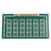
This double-sided FR4 TG170 PCB is a versatile and cost-effective solution. It suits applications from industrial control systems to consumer electronics and medical devices. С толщиной 1,6 мм, 1OZ copper layers, and a lead-free HAL surface finish, this PCB balances mechanical strength, electrical reliability, and environmental compliance. Поэтому, it is ideal for mid-complexity electronics requiring consistent performance at scale.
Constructed from FR4 material with a high glass transition temperature (Тг) 170 ° C., this PCB offers enhanced thermal stability. Compared to standard FR4 (Тг130°С), it performs better in environments with temperature fluctuations between -20°C and +80°C. This advantage ensures reliable operation. The double-sided design also allows engineers to route complex circuits efficiently. Dual-layer signal traces and copper pours for power and ground planes reduce electromagnetic interference (Эми) and improve signal integrity. Как результат, it supports low-to-medium-speed applications such as microcontrollers, sensor interfaces, и модули связи.
Lead-Free HAL Surface Finish: This finish is RoHS and REACH compliant. It provides excellent solderability and good corrosion resistance. Кроме того, it suits both manual and automated assembly, especially in applications requiring frequent rework.
1Медные слои OZ: With 35μm thickness, the copper layers support moderate current loads up to 8A per wide trace. They enable fine-line routing with minimum line/space of 100μm/100μm. This balances power delivery and high component density.
Зеленая паяльная маска LPI: The solder mask enhances visual clarity for assembly and rework. Более того, it resists common industrial contaminants like oils, solvents, и чистящие средства. Поэтому, it is ideal for harsh environments such as manufacturing plants or outdoor equipment.
The PCB undergoes precise fabrication to guarantee quality and reliability:
High-precision mechanical drilling with ±50μm tolerance ensures accurate vias.
Plated Through Holes (Пт) receive 25-35μm copper coating for strong inter-layer connections.
UV lithography defines fine circuit patterns with 100μm resolution.
Tin plating protects conductive traces during etching.
Durable green LPI solder mask is cured at 150°C.
100% Электрические испытания (Электронный тест) verifies continuity and isolation.
Автоматическая оптическая проверка (Аои) checks solder mask coverage and detects defects.
Defective panels are strictly rejected, ensuring only flawless PCBs ship to customers.
Industrial Control: Suitable for PLC modules, relay control boards, and sensor interfaces prioritizing reliability and cost-efficiency.
Потребительская электроника: Supports low-power smart devices, носимые устройства, and audio modules with compact designs and accessible test points.
Медицинские устройства: Compliant with RoHS, it fits diagnostic and monitoring equipment requiring stable performance.
Prototyping & Education: Popular for rapid prototyping due to compatibility with standard SMT/DIP components.
Соответствует классу IPC-6012 2 standards for industrial applications.
Fully RoHS/REACH compliant.
Tested for thermal stress (260°C reflow) and vibration resistance (5-500Гц).
By combining a high-Tg substrate, lead-free HAL finish, and double-sided design, this PCB delivers a reliable, scalable, and cost-effective platform. Engineers developing industrial, consumer, or medical electronics will find this solution dependable and compliant with global standards.