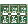
8-Печатная плата слоя FR4 разработана для электронных устройств высокой плотности, требующих баланса целостности сигнала, Распределение энергии, и компактные форм-факторы, например, бытовая электроника, медицинское оборудование, и модули промышленного управления. А 8-архитектура слоя (обычно 4 Слои сигнала + 4 Силовая/основные плоскости) обеспечивает сложную маршрутизацию компонентов с мелким шагом, сводя к минимуму электромагнитные помехи (Эми). А 1.2MM Толщина доски предлагает легкий, но жесткий фундамент, идеально подходит для приложений с ограниченным пространством, где вес и долговечность имеют решающее значение.
Построен с FR4 материал, печатная плата обеспечивает надежную электрическую изоляцию (Диэлектрическая постоянная εr = 4,5) и механическая стабильность, подходит для широкого спектра рабочих сред. А 2Унция (70мкм) толщина меди на всех слоях увеличивает токонесущую способность (до 15А за след) сохраняя при этом гибкость конструкции как для силовых, так и для сигнальных трасс.. А Зеленый ИЛПИ (Жидкость) паяльная маска не только защищает схему от вредного воздействия окружающей среды, но и повышает точность визуального контроля, Пока Белый шелкосный экран обеспечивает четкую маркировку и обозначения компонентов для сборки и обслуживания.
Ключевой особенностью является Соглашаться (Электролетное никелевое погружение) обработка поверхности, что обеспечивает плавность, коррозионностойкая отделка для превосходной паяемости. Слой никеля (3–5 мкм) добавляет долговечность, И золотой слой (0.05–0,1 мм) предотвращает окисление, что делает его пригодным для длительного использования. А Пофв (Нанесенный на заполненные уклоны) технология еще больше повышает надежность печатной платы: переходные отверстия заполнены проводящим материалом и покрыты, устранение пустот, которые могут вызвать термическое напряжение или растекание припоя. Это особенно важно для конструкций с высокой плотностью размещения компонентов с малым шагом. (НАПРИМЕР., 0.5BGA с шагом мм) и обеспечивает стабильную производительность в процессах пайки оплавлением.
Производство этой печатной платы включает в себя передовые технологии, обеспечивающие точность и качество.:
- Лазерная прямая визуализация (LDI) обеспечивает высокую точность линий (Минимальная ширина линии/пространство: 50мкм/50 мм) для сложной маршрутизации.
- обработка ПОФВ использует проводящую эпоксидную смолу или смолу для заполнения переходных отверстий, с последующим нанесением покрытия для создания гладкой поверхности.
- 100% Аои (Автоматическая оптическая проверка) проверяет покрытие паяльной маски и четкость шелкографии.
- Электрические испытания обеспечивает непрерывность и сопротивление изоляции, Встреча с IPC-6012 2 стандарты.
Инженеры оценят универсальность печатной платы при работе как с маршрутизацией сигналов с высокой плотностью, так и с приложениями с умеренным энергопотреблением.. В потребительской электронике, он поддерживает компактные конструкции для смартфонов, таблетки, и носимые устройства, где пространство в дефиците. В медицинских приборах, технология POFV и отделка ENIG способствуют долгосрочной надежности диагностического оборудования.. В промышленных системах, медь плотностью 2 унции и материал FR4 обеспечивают долговечность, необходимую для панелей управления и модулей автоматизации..
Выбрав эту 8-слойную печатную плату FR4 с медью толщиной 2 унции, Загадка финишировать, и технология POFV, клиенты получают решение, которое уравновешивает плотность, надежность, и экономическая эффективность. Его сочетание передовых возможностей наполнения, обработка поверхности премиум-класса, а точность изготовления делает его стратегическим выбором для приложений, где интеграция компонентов и долгосрочная производительность имеют решающее значение.. Окреплен ISO 9001:2015 сертификация, эта печатная плата обеспечивает стабильное качество от прототипирования до массового производства.

")