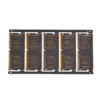
This 6 – layer FR4 TG170 PCB is a meticulously engineered solution tailored for the demanding automotive industry, backed by the prestigious IATF16949 certification. In the automotive field, reliability and performance are nonnegotiable, and this PCB rises to the challenge with its advanced features and highquality construction.

1. Material and Structural Advantages

  • FR4 TG170 Material: Constructed from FR4 material with a glass transition temperature (Tg) of 170°C, it offers superior thermal stability. In automotive applications, where components are often exposed to elevated temperatures, especially in the engine compartment or during longdistance driving, this highTg material ensures that the PCB remains dimensionally stable. It reduces the risk of warping, delamination, and electrical performance degradation, which are critical issues in automotive electronics. For example, in automotive ADAS (Advanced DriverAssistance Systems) where sensors and processing units generate heat, the TG170 material can effectively withstand the heat without compromising the integrity of the board.
  • 1.6mm Board Thickness: With a 1.6mm thickness, the PCB strikes a balance between mechanical strength and weight. In automotive design, where space and weight are carefully optimized, this thickness provides enough rigidity to withstand vibrations and mechanical shocks during vehicle operation. At the same time, it is not overly heavy, which is crucial for maintaining fuel efficiency and overall vehicle performance.
  • 1OZ Copper on All Layers: All layers are fabricated with 1OZ (35мкм) copper, which provides excellent electrical conductivity. This thickness is suitable for handling the electrical currents required in automotive circuits, whether it’s powering sensors, actuators, or communication modules. The 1OZ copper also enables fineline routing (with a minimum line/space of 75μm/75μm), allowing for highdensity component placement, a common requirement in modern automotive electronics where more functionality is being packed into smaller spaces.

2. Surface Finish and Solder Mask

  • ENIG Surface Finish: The Electroless Nickel Immersion Gold (Соглашаться) surface finish is a key feature of this PCB. А 3 – 5μm nickel barrier layer effectively prevents copper oxidation, Пока 0.05 – 0.1μm gold layer on top ensures excellent solderability and wirebonding compatibility. In the automotive environment, where connectors are frequently mated and unmated, and components need to maintain reliable electrical connections over long periods, the ENIG finish provides the necessary durability and corrosion resistance.
  • Black Solder Mask: The black solder mask not only enhances the aesthetic appearance of the PCB but also offers practical benefits. It provides better visual contrast for component identification, which is useful during assembly and maintenance. Additionally, the black solder mask has superior UV resistance, which is important for automotive applications where the PCB may be exposed to sunlight, especially in vehicles with transparent covers or in outdooruse automotive electronics.

3. Special Features for Automotive Applications

  • BGA Support: Ball Grid Array (BGA) components are increasingly used in automotive electronics for their highdensity packaging and excellent electrical performance. This PCB is designed to support BGA components, with optimized layout and vias to ensure reliable connections. The PCB’s manufacturing process is carefully controlled to meet the tight tolerances required for BGA soldering, reducing the risk of solder joint failures, which can be catastrophic in automotive systems.
  • Outline Routing: The PCB undergoes precise outline routing, achieving tight mechanical tolerances (±0.1mm). This is essential for automotive applications as it ensures a perfect fit within the vehicle’s enclosures. The smooth, burrfree edges produced by outline routing also contribute to the overall durability of the PCB, protecting it from damage during installation and operation in the rugged automotive environment.

4. Manufacturing Process and Quality Assurance

  • Rigorous Manufacturing Process: The PCB is fabricated through a comprehensive process. Starting with innerlayer processing, laser direct imaging (LDI) is used to define 75μm traces on 1OZ copper cores, followed by etching to form the inner circuitry. Highprecision mechanical drilling creates vias with ±50μm accuracy, which are then coated with electroless and electrolytic copper to achieve a uniform 35μm thickness for robust throughhole connections. After dryfilm lamination and UV exposure to define the outerlayer traces, tin plating protects conductive areas during etching. Finally, the ENIG surface finish is applied after soldermask curing.
  • IATF16949Compliant Quality Control: Being IATF16949 certified means that the entire manufacturing process, from raw material sourcing to final product inspection, adheres to the strict quality management system requirements of the automotive industry. Every board undergoes 100% electrical testing (Etest) to verify continuity (≤0.1Ω) and isolation (≥100MΩ). Xray inspection checks via integrity, and automated optical inspection (Аои) ensures soldermask coverage, trace quality, and overall board quality. Xout panels are strictly rejected, ensuring that only defectfree PCBs are delivered to automotive customers.

5. Applications in the Automotive Field

  • Advanced DriverAssistance Systems (ADAS): In ADAS, which includes functions such as collision avoidance, lanekeeping assist, and adaptive cruise control, this PCB can be used to integrate sensors (like cameras, radar, and lidar), processing units, and communication modules. The highspeed signal routing capabilities of the 6 – layer design, along with its thermal stability, are crucial for the realtime data processing and reliable operation required in ADAS.
  • Infotainment Systems: For invehicle infotainment systems that provide navigation, audio, and video services, the PCB’s ability to support highdensity component placement and its reliable electrical performance are essential. The BGA support allows for the integration of powerful processors and memory modules, while the ENIG finish ensures longlasting connectivity for various input and output interfaces.
  • Powertrain Control: In powertrain control systems that manage the engine, transmission, and other powerrelated components, the PCB’s robustness against vibrations, thermal stability, and highcurrenthandling capabilities (thanks to 1OZ copper) make it an ideal choice. The IATF16949 certification also gives automotive manufacturers confidence in the quality and reliability of the PCB in this critical application area.


In summary, this 6 – layer FR4 TG170 PCB, with its suite of advanced features, highquality manufacturing process, and IATF16949 certification, is a toptier solution for automotive applications, providing the reliability, performance, and quality demanded by the automotive industry.

Возможность печатной платы


Элемент Стандартная печатная плата Индивидуальная печатная плата
Количество слоев 2-20 2-50
Материал FR4 Hi Speed ​​Material от Taiwan Union, И технология, Высокочастотный материал от Роджерса и т. Д..
Толщина печатной платы 0.4-3.2мм 0.4-6.4мм
Медный вес Принесите-3o Принесите 10
Мин. Диаметр отверстия 0.3мм 0.1мм от лазерной тренировки
Размер печатной платы Мин. 6.00X6.00 мм макс. 600.00X620,00 мм
Печата финиш Отстранение, Hal-Leadfree, Соглашаться, Enepic, Погружение, Погружение серебро, Оп
Мин. 4мил за 1 унцию 2.5мил за 1 унцию
Тип преорета 2116,1080 2116,1080,7628,3313,106
Min.width/пространство 4/4 мил 2.5/2.5 мил
Мин. Кольцевое кольцо 4/4 мил 2.5/2.5 мил
Соотношение сторон 8:1 15:1
Время выполнения 2 недели 5 Дни - 5 Недели
Импеданс терпимость ±5% - ±10% ±5% - ±10%
Другие методы Золотые пальцы, Слепые и похороненные отверстия, Отчитываемая паяная маска, Кравление, Углеродная маска, HOLERSICK HOLE,
Половина/Кастелленная дыра, Нажмите отверстие для подключения, Через подключенную/заполненную смолой, Через Pad (VIP, Пофв), Многофинансы на одной печатной плате

Он будет закрыт в 0 секунд

Возможность PCBA


Нет. Элемент Параметр возможностей процесса
1 Количество заказа Более 1 шт
2 Тип печатной платы Жесткая печатная плата, FPC, Жесткая пласка
3 Ассамблея Пост, Это, Смешанная технология или поп
4 Компонентный источник Полный под ключ, Частичный под ключ, Отправлено
5 Размер печатной платы 45*45мм -- 510*500мм
6 BGA Package BGA ее. 0.14мм, BGA 0,2 мм шаг
7 Презентация деталей Лента, Катушка, Палка или поднос
8 Проволока & Кабель Проволочная жгут и кабельная сборка
9 Качественная проверка Визуальный, SPI, Фей, Аои; Рентгеновская проверка
10 Точность монтажа ±0.035мм (±0.025мм)
11 Мин пакет 01005 (0.4мм*0,2 мм)
12 Конформное покрытие Доступно на машине
13 IC Inspection Функция, Электрический тест или DECAP
14 Время выполнения 3 дни - 5 Недели
15 Другие методы Сборка коробки сборка, IC программирование, Компоненты стоимость, Функция & Испытание на старение как пользовательский,
Нажмите Fit Assembly, SAC305 или лучшая паяная паста используется, BGA REBALLING или REWORD,
Узел крышки щита для контроля эмиссии EMI

Он будет закрыт в 0 секунд

Возможность FPC


Нет. Элемент Параметр возможностей процесса
1 Количество слоев 1-8 Слои
2 Материал FPC Пик, ДОМАШНИЙ ПИТОМЕЦ, РУЧКА, FR-4
3 Окончательная толщина 0.06-4.0мм
4 Размер доски 250.00X1200 мм
5 Медная фольга 12один,18один,35один,70один
6 Мин ширина/пространство 3тысяча/3 мили
7 HOLEWALL CODINGE 8-20мкм
8 Поверхностная обработка Холл Лидерри, Соглашаться, Погружение серебро/олово, Оп
9 Определяет измерение ± 2 мили
10 Припаяя теплостойкость 280℃ / 10секунды
11 Тип жесткости Пик, FR4, Нержавеющая сталь, Алюминий
12 Мин. День дыры (Пт) 0.1мм ± 3 мили
13 Мин. День дыры (Npth) 0.25± 2 мили
14 Макс/мин толщины солдата 2Мил/0,5 млн (50Один/12,7 мм)
15 Мин слот 0.8мм × 1 мм

Он будет закрыт в 0 секунд