
Prototype PCB Assembly: A Comprehensive Guide
Prototype PCB Assembly refers to the process of assembling a printed circuit board (PCB) that is in its prototype stage. This assembly occurs during the early phases of product development to validate the design and functionality of the PCB before it moves into mass production. It is a critical step in the development lifecycle, as it allows engineers to test the design, identify potential issues, and make necessary adjustments to ensure the product’s performance and reliability.
1. Definition and Purpose
Prototype PCB Assembly is the process of assembling a circuit board that is being tested for the first time. This typically involves soldering various electronic components, such as resistors, capacitors, integrated circuits (ICs), connectors, and microchips, onto a PCB that has already been designed and fabricated. The purpose of this assembly is to:
-
Verify the Design: Ensure that the circuit functions correctly and that all components are positioned correctly.
-
Test Functionality: Confirm that the PCB operates as intended under real-world conditions.
-
Identify Design Flaws: Spot potential issues with the electrical, mechanical, or thermal performance of the PCB before scaling up to full production.
The prototype PCB is usually assembled in small quantities to facilitate testing and modification before committing to large-scale manufacturing.
2. The Prototype PCB Assembly Process
The process of Prototype PCB Assembly involves several steps, which are crucial for ensuring that the final product meets both design specifications and performance expectations.
2.1 Design and Fabrication of the PCB
-
Schematic Design: Engineers design the schematic diagram, representing the electrical connections between components.
-
PCB Layout: Once the schematic is ready, engineers use PCB design software (such as Altium Designer or Eagle) to place the components and route the electrical traces. The layout must adhere to specific electrical and mechanical constraints.
-
Fabrication: The design is transferred to a physical PCB through a process of etching, layering, and patterning. The fabricated PCB is inspected for defects, and any manufacturing issues are corrected before moving to the assembly stage.
2.2 Component Sourcing
-
Component Selection: Depending on the design, components are selected based on their specifications (voltage, size, power rating, etc.), availability, and cost.
-
Prototyping Components: In prototype stages, components may be manually sourced, including off-the-shelf components or specially ordered parts for custom needs.
-
Component Procurement: Once components are selected, they are procured in smaller quantities (usually for the prototype) to assemble the PCB.

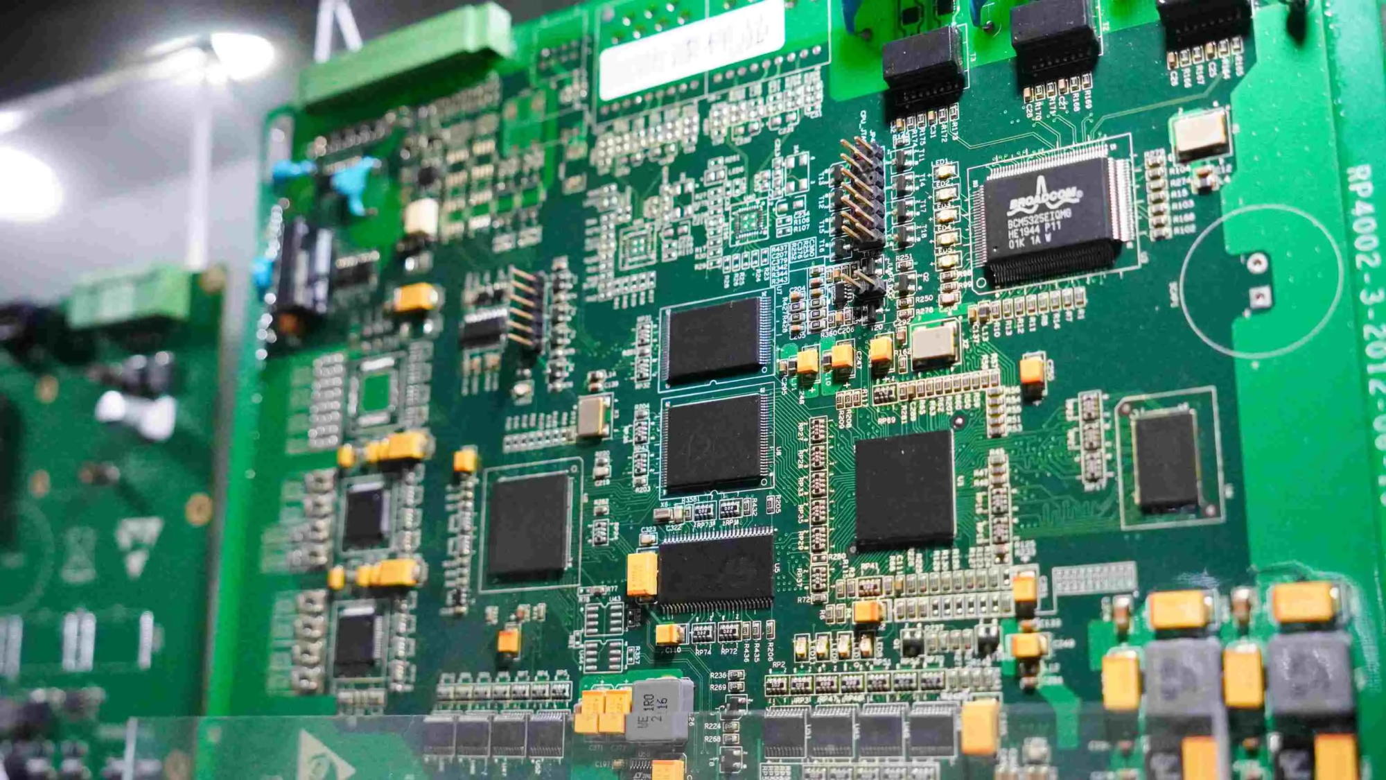
2.3 PCB Assembly
-
Surface-Mount Technology (SMT): Small components such as resistors, capacitors, and ICs are placed on the surface of the PCB, which is then heated in a reflow oven to solder the components in place.
-
Through-Hole Technology (THT): Larger or more robust components are inserted into drilled holes in the PCB and soldered on both sides.
-
Manual Assembly: For highly customized or intricate components, manual assembly techniques are employed, especially for small-scale or prototype production runs.
-
Inspection: After assembly, the prototype PCB undergoes inspection to verify that components are properly soldered and positioned. Techniques like Automated Optical Inspection (AOI) or X-ray inspection may be used to detect defects.
2.4 Testing and Debugging
-
Electrical Testing: Functional testing ensures that electrical connections work as intended, checking for short circuits, continuity, and voltage stability.
-
Functional Verification: The assembled prototype PCB is connected to power and peripherals to ensure the circuit performs the desired functions.
-
Thermal Testing: Identifying heat-related issues such as overheating components or inadequate heat dissipation.
-
Debugging: Engineers use tools like oscilloscopes, logic analyzers, and multimeters to debug issues such as signal interference, incorrect voltage, or malfunctioning components.
2.5 Iteration and Refinement
After testing, the results are analyzed. If issues are found, modifications are made to the design or assembly process. This step may involve:
-
Re-designing the PCB: Fixing design flaws or optimizing the layout.
-
Component Changes: Accommodating new specifications or using alternative components.
-
Re-assembly and Retesting: Validating the modified design through further testing.
3. Key Benefits of Prototype PCB Assembly
-
Design Validation: Validates the circuit design before mass production, reducing later-stage production issues.
-
Early Problem Detection: Identifies and addresses design flaws, component incompatibilities, and manufacturing issues early.
-
Faster Time-to-Market: Enables faster iterations and refinements, accelerating the product development cycle.
-
Cost Efficiency: Saves money by addressing issues early, preventing costly design changes after production.
-
Customization and Flexibility: Offers high flexibility for design adjustments, component modifications, and feature testing.
4. Applications of Prototype PCB Assembly
Prototype PCB assembly is widely used in various industries, including:
-
Consumer Electronics: Essential for products like smartphones and home appliances.
-
Automotive: Used in infotainment systems, navigation, safety systems, and sensors.
-
Medical Devices: Critical for testing components used in life-saving equipment.
-
Industrial Equipment: Important for machinery, robotics, and automation.
-
Telecommunications: Key in designing and testing networking equipment.
5. Challenges in Prototype PCB Assembly
-
Component Sourcing: Difficulty sourcing components, leading to potential delays.
-
Design Complexity: Complex designs (e.g., multi-layer PCBs) can be challenging.
-
Cost of Prototyping: Low-quantity custom PCBs and component sourcing can be expensive.
-
Testing and Debugging: Debugging can be time-consuming and require specialized tools.
6. Conclusion
Prototype PCB Assembly is a crucial phase in the electronics development process. It helps engineers test, validate, and refine designs before committing to mass production. By identifying issues early, it reduces manufacturing errors, accelerates development, and saves money.