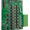
8-layer PCB is engineered for mission-critical industrial communication applications, where high-frequency signal integrity, electromagnetic compatibility (EMC), and rugged durability are essential. With dimensions of 190mm×170mm and a 1.7mm thickness, the board balances large-scale component integration with mechanical stability for industrial control cabinets and communication hubs. The unique TU-862+RO4350B material stackup combines TU-862’s cost-effective mechanical strength with RO4350B’s low-loss dielectric properties (Dk=3.48, tanδ=0.004 at 10GHz), making it ideal for high-speed data transmission in protocols like Ethernet, CANopen, and PROFIBUS.
- Asymmetric Copper Thickness:
- Outer layers: 1OZ (35μm) for robust power traces and EMI shielding
- Inner layers: 0.5OZ (18μm) for fine-pitch signal routing
- Enables balanced power distribution (4 power/ground planes) and high-speed signal layers (4 differential pair channels)
- Precision Impedance Control:
- 50Ω ±8% for microstrip/stripline configurations
- Achieved via controlled dielectric thickness and trace width calculations
- Minimizes signal reflection in 10Gbps Ethernet and industrial wireless interfaces
- Non-Conductive Filled Vias (NCFV) with Copper Capping:
- Vias filled with resin to prevent voids, then capped with copper for smooth surface finish
- Eliminates solder wicking risks in BGA areas and improves thermal conductivity
- Sequential Lamination:
- 8 layers laminated in stages to ensure uniform dielectric thickness and registration accuracy (<50μm)
- ENIG Surface Finish:
- 3-5μm nickel layer for corrosion resistance
- 0.05-0.1μm gold layer for long-term solderability
- Matt Green LPI Solder Mask:
- Reduces glare during AOI inspection
- Provides superior chemical resistance in industrial environments
- EMC/EMI Mitigation:
- Ground plane stitching vias placed at intervals of 2mm to suppress common-mode noise
- Precision differential pair routing with length matching controlled to within 5 mils (0.127mm) to ensure minimal signal skew
- Thermal Management:
- Thermal vias connecting power planes to outer layers for efficient heat dissipation
- Copper pour areas on power layers to reduce hotspots
- Mixed Assembly Support:
- SMT for high-density ICs (e.g., PHY chips, FPGAs)
- DIP for rugged connectors (e.g., RJ45, DB25) and relays
- 100% Automated Testing:
- Impedance verification per layer
- X-ray inspection of NCFV vias
- AOI for solder mask and silkscreen quality
- Environmental Testing:
- Temperature cycling (-40°C to +85°C, 1,000 cycles)
- Vibration testing (5-500Hz, 2G acceleration)
- Standards Compliance:
- IPC-6012 Class 3 for mission-critical applications
- RoHS/REACH for hazardous substance restrictions
- EN 55032 Class A for electromagnetic emissions
- Industrial Ethernet Switches:
Supports 10GBASE-T and PoE+ with minimal signal degradation
- Wireless Base Stations:
Enables 5G NR sub-6GHz radio frequency routing
- PLC & SCADA Systems:
Facilitates real-time data exchange in manufacturing plants
- Railway Communication Networks:
Meets EN 50155 environmental standards for rolling stock applications

")