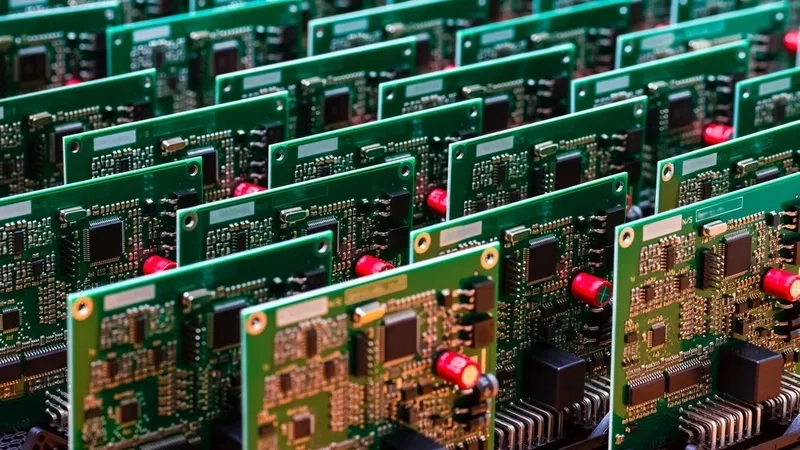
PCB Design and Layout
Printed Circuit Board (PCB) design has evolved into a highly specialized discipline within the electronics industry. PCBs are essential because they:
-
Provide electrical interconnections between components
-
Offer rigid structural support for mounting components
-
Deliver a compact, reliable package for integration into end products
They are the foundation of modern electronic devices, enabling advanced semiconductors to communicate at ultra-high data speeds and ensuring both form and function.
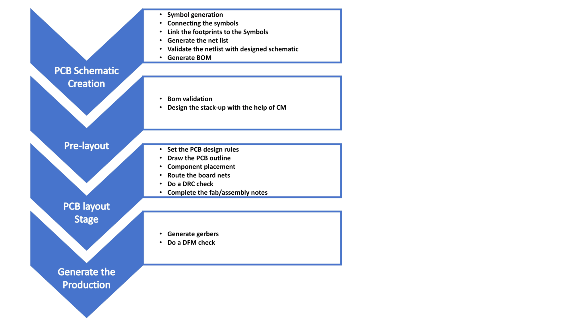
Normal Steps in PCB Design
Below is a step-by-step guide to the typical PCB design process, beginning from schematic creation to final material preparation.
Step 1: PCB Schematic Creation
This is the conceptual and planning phase of the design process:
🧩 Key Tasks:
-
Schematic Symbol Generation & Placement
Create digital representations of components and place them in your design software. -
Pin Numbering
Ensure all pins are numbered and correspond to the actual component datasheet. -
Reference Designators
Assign unique codes like R1, C2, U3 to identify each component on both the Bill of Materials (BOM) and the silkscreen layer in Gerber files. -
Assigning a Footprint
Link each schematic symbol to its correct PCB footprint to ensure physical compatibility. -
Connecting the Symbols
Draw the logical connections between components using wires or nets. -
Link Footprints to Symbols
Verify that each schematic symbol correctly corresponds to a footprint for layout. -
Generate the Netlist
Create a file that defines all electrical connections, essential for PCB layout. -
Perform Netlist Check
Run a Design Rule Check (DRC) to ensure there are no missing or conflicting connections. -
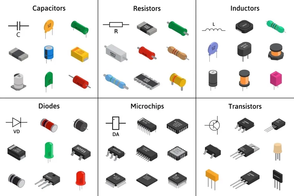
Generate the BOM (Bill of Materials)
A detailed list of all components used, including:-
Part numbers
-
Quantity
-
Package type
-
Manufacturer
-
💡 Tip:
Before generating the BOM, choose components that are readily available and cost-effective from the market. Carefully balance between:
💰 Material Cost
⚙️ Component Functionality
This helps ensure manufacturability, cost control, and reliability from the very beginning.
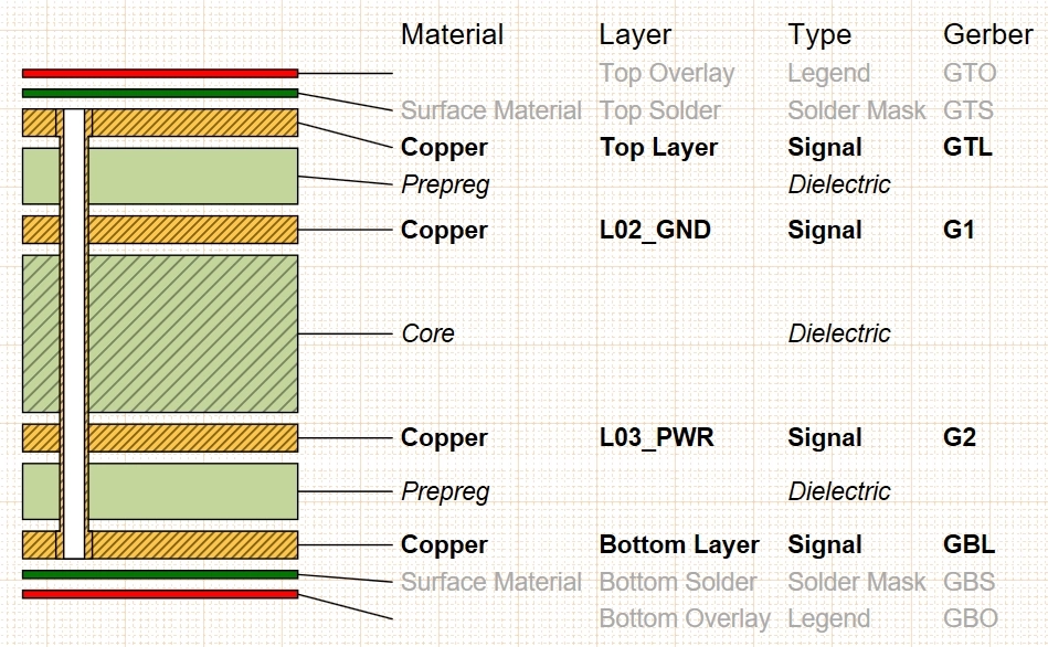
Step 2: Pre-layout stage
- BOM validation
- Design the stack-up and confirmed with PCB manufacturer

Step 3: PCB layout stage
- Setting up the stack-up
- Set the PCB design rules
- Draw the PCB outline
- Component placement
- Route the board nets
- Perform a design rule check (DRC)
- Complete PCB fab/assembly notes

Step 4: Generate the production files
- Gerber and drill files
- BOM
- Pick and Place file
- Assembly Drawings
- Firmware files (if needed)
PCB designer should take time to learn the basics of PCB manufacturing so that they can ensure their designs are fully manufacturable. This relates to an important set of practices that should be built into your design process, known as design for manufacturing (DFM). Take some time to learn about some basic design mistakes that can derail manufacturing and cause your board to be sent back to you for redesigns before production.
Simulation Tools for PCB Design
Simulation tools play a crucial role in the PCB design process. They allow engineers to predict performance, identify potential issues, and optimize circuit behavior before entering costly manufacturing stages. Below are the key simulation types used during PCB design:
Signal Integrity Simulations
Signal integrity (SI) simulations analyze the quality of signals traveling through PCB traces. These simulations help detect:
-
Reflections
-
Crosstalk
-
Signal attenuation
Such issues are critical in high-speed digital circuits. Early detection allows engineers to adjust:
✔ Layout
✔ Trace routing
✔ Termination strategies
Ensuring reliable signal performance.
Power Distribution Simulations
Power distribution simulations evaluate voltage and current behavior across the PCB. They help identify:
-
Voltage drops
-
High current density areas
-
Potential thermal hotspots
By optimizing the Power Distribution Network (PDN), you can:
✅ Increase efficiency
✅ Reduce heat generation
✅ Improve system reliability
Thermal Simulations
Thermal simulations are essential for predicting temperature distribution across the board. They consider:
-
Component power dissipation
-
Ambient conditions
-
Heat transfer methods
These simulations help in identifying hotspots and improving thermal management by:
🔥 Adding thermal vias
🔥 Enlarging copper areas
🔥 Using heat sinks or thermal pads
Integrated Simulation Tools
Most modern PCB design platforms support integrated simulation environments, enabling quick iterations without switching tools.
Popular tools include:
-
SPICE (Simulation Program with Integrated Circuit Emphasis) -
HyperLynx by Mentor Graphics -
Ansys SIwave
These tools provide multi-domain analysis to meet various design complexities.
By leveraging simulation tools early and often, designers can reduce errors, increase performance, and ensure product reliability—before a single board is built.

At Fully Hong Electronics, PCB Design Service includes:
- An initial consultation to discuss your design is always free.
- We can help you select the right parts for your PCB design.
- We can take your schematic in any form and convert it into the CAD format you need.
- We will create Altium schematic symbols and PCB footprints for each part in your design.
- After completing the schematic diagram, we will submit it for your review.
- We will create a PCB outline and do a preliminary placement of all parts.
- Upon your approval of the parts placement, we will continue with the detailed PCB layout.
PCB FABRICATION
- PCB prototypes or mass production boards with fast lead time
- You can have high quality PCB with very competitive price at Fully Hong Electronics
PCB ASSEMBLY
- Use the latest SMT & Through-hole Technology.
- One-stop solution from PCB design, PCB fabrication to PCB assembly etc.
- You can get PCBA offer includes PCB, component and assemblycost within 2-3 days
- Fast PCBA lead time: 3-4 weeks, it includes the time to purchase all components