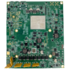
8-레이어 FR4 PCB: 산업용 통신을 위한 핵심 보드
이 8레이어 FR4 PCB는 까다로운 산업용 통신 애플리케이션을 위해 특별히 설계되었습니다., 산업용 제어 캐비닛을 위한 안정적이고 신뢰할 수 있는 기반 제공, 통신 게이트웨이, 및 자동화 시스템. 치수와 함께 174.52×121.25mm 그리고 두께 1.6mm, 이 보드는 기계적 안정성과 다수의 중요 구성 요소를 통합하는 기능 사이의 균형을 유지합니다.. 뛰어난 신호 무결성부터 내구성 있는 빌드까지, 이 PCB는 진동이 있는 열악한 환경에서도 안정적인 성능을 제공하도록 설계되었습니다., 온도 변동, 및 전자기 간섭.
주요 기술적 기능
1. 고급 스택업 및 신호 무결성
- 8-레이어 스택 업: 이 설계에는 4개의 신호 레이어와 4개의 전력/접지 평면이 있습니다.. 이 아키텍처는 EMI를 효과적으로 억제합니다. (전자기 간섭) 이더넷 및 CANopen과 같은 고속 차동 쌍에 최적화된 라우팅 경로를 제공합니다..
- 정밀 임피던스 제어: 차동 라인 임피던스는 다음과 같이 제어됩니다. 100오±8%, 단일 종단 라인 임피던스는 다음에서 제어됩니다. 50오±8%. 이는 신호 반사를 최소화하고 기가비트 이더넷과 같은 고속 인터페이스의 무결성을 보장합니다..
- 1온스 (35μm) 구리 두께: 구리 두께는 미세 라인 라우팅 요구 사항의 균형을 유지합니다. (최소 선/공간: 75μm/75μm) 최대 10A의 높은 전류 전달 용량, 고전력, 고밀도 설계 지원.
2. 산업 등급 설계 및 제조
- 동의하다 (전기 전기 니켈 몰입 금) 표면 마감: 마무리는 니켈 층을 제공합니다 4-6μm 그리고 금층 0.05–0.1mm. 니켈층은 우수한 내식성을 제공합니다., 금층은 장기적인 납땜성과 와이어 본딩 호환성을 보장합니다., 신뢰성을 보장, 오래 지속되는 연결.
- 블루 LPI 솔더 마스크: The blue ink not only effectively protects circuitry and prevents oxidation but also provides excellent visual differentiation in complex systems, making identification and maintenance easier.
- Mixed Assembly Compatibility: The board supports both smt (표면 실장 기술) for high-density ICs (예를 들어, PHY 칩, FPGA) 그리고 담그다 (Dual In-line Package) for rugged connectors (RJ45, DB25) 그리고 릴레이, combining high integration with durability.
- High-Precision Manufacturing: We use LDI (레이저 직접 이미징) technology for 75μm trace accuracy. The electrolytic copper plating process ensures thickness uniformity within ±5%, guaranteeing consistent trace performance.
Quality and Compliance
- Comprehensive Quality Control:
- 100% 전기 테스트 (e- 테스트): This ensures the continuity of all circuits during the manufacturing stage.
- 자동화 된 광학 검사 (AOI): Used to detect defects on the bare board, such as shorts and opens.
- 엑스레이 검사: 보이드나 브리지가 없는지 확인하기 위해 BGA 패키지의 솔더 조인트 품질을 검증합니다..
- 환경 및 산업 표준:
- 준수 IPC-6012 클래스 2 산업 응용 분야의 표준.
- RoHS 준수/도달 인증됨, 유해물질 제한 준수.
- ISO 9001:2015 인증됨, 품질 관리 시스템에 대한 보증 제공.
일반적인 애플리케이션
- 산업용 이더넷 네트워크: 낮은 지연 시간 제공, 10/100/1000Mbps 이더넷 통신을 위한 저지터 고속 전송 플랫폼.
- PLC & SCADA 시스템: 제조 시설 내 실시간 데이터 교환 및 제어 지원.
- 철도 통신 시스템: 준수 안에 50155 기준, 열악한 철도 환경에서도 안정적인 작동 보장.
- 무선 기지국: 5G sub-6GHz 및 Wi-Fi를 위한 안정적인 RF 신호 라우팅 제공 6 응용 프로그램.
정밀한 스택업 설계로, 우수한 전기적 성능, 강력한 산업 등급 기능, 이 PCB는 고성능 구축을 위한 이상적인 선택입니다., 신뢰성이 높은 산업용 통신 시스템.