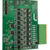
8-레이어 PCB는 미션 크리티컬 산업 통신 애플리케이션용으로 설계되었습니다., 고주파 신호 무결성, 전자기 호환성 (EMC), 그리고 견고한 내구성은 필수입니다. 치수와 함께 190mm×170mm 그리고 a 1.7MM 두께, 이 보드는 산업용 제어 캐비닛 및 통신 허브를 위한 기계적 안정성과 대규모 구성 요소 통합의 균형을 유지합니다.. 독특한 TU-862+RO4350B 재료 스택업 TU-862의 비용 효율적인 기계적 강도와 RO4350B의 저손실 유전 특성을 결합합니다. (Dk=3.48, 10GHz에서 tanδ=0.004), 이더넷과 같은 프로토콜의 고속 데이터 전송에 이상적입니다., CANopen, 그리고 프로피버스.
- 비대칭 구리 두께:
- 외부 레이어: 1온스 (35μm) 견고한 전력 트레이스 및 EMI 차폐용
- 내부 레이어: 0.5온스 (18μm) 미세 피치 신호 라우팅용
- 균형 잡힌 전력 분배 가능 (4 전원/지상 비행기) 및 고속 신호 레이어 (4 차동 쌍 채널)
- 정밀 임피던스 제어:
- 50마이크로 스트립/스트립 라인 구성의 경우 ω ± 8%
- 제어된 유전체 두께 및 트레이스 폭 계산을 통해 달성
- 10Gbps 이더넷 및 산업용 무선 인터페이스에서 신호 반사를 최소화합니다.
- 비전도성 충진 비아 (NCFV) 구리 캡핑 포함:
- 보이드를 방지하기 위해 수지로 채워진 비아, 그런 다음 매끄러운 표면 마감을 위해 구리로 덮습니다.
- BGA 영역의 납땜 위킹 위험을 제거하고 열 전도성을 향상시킵니다.
- 순차적 적층:
- 8 균일한 유전체 두께와 등록 정확도를 보장하기 위해 단계별로 적층된 레이어 (<50μm)
- ENIG 표면 마감:
- 3-5내식성을 위한 μm 니켈층
- 0.05-0.1장기간 납땜성을 위한 μm 금층
- 매트 그린 LPI 솔더 마스크:
- AOI 검사 중 눈부심을 감소시킵니다.
- 산업 환경에서 우수한 내화학성을 제공합니다.
- EMC/EMI 완화:
- 공통 모드 노이즈를 억제하기 위해 2mm 간격으로 배치된 접지면 스티칭 비아
- 길이 일치가 내부로 제어되는 정밀 차동 쌍 라우팅 5 밀스 (0.127mm) 신호 왜곡을 최소화하기 위해
- 열 관리:
- 효율적인 열 방출을 위해 전원 평면을 외부 레이어에 연결하는 열 비아
- 핫스팟을 줄이기 위해 전원 레이어의 구리 주입 영역
- 혼합 조립 지원:
- 고밀도 IC용 SMT (예를 들어, PHY 칩, FPGA)
- 견고한 커넥터용 DIP (예를 들어, RJ45, DB25) 그리고 릴레이
- 100% 자동화된 테스트:
- 레이어별 임피던스 검증
- NCFV 비아의 X선 검사
- 솔더 마스크 및 실크스크린 품질을 위한 AOI
- 환경 테스트:
- 온도 순환 (-40° C ~ +85 ° C, 1,000 사이클)
- 진동 테스트 (5-500HZ, 2G 가속)
- 표준 준수:
- IPC-6012 클래스 3 미션 크리티컬 애플리케이션 용
- 유해 물질 제한에 대한 RoHS/REACH
- 안에 55032 전자기 방출에 대한 클래스 A
- 산업용 이더넷 스위치:
신호 저하를 최소화하면서 10GBASE-T 및 PoE+ 지원
- 무선 기지국:
5G NR sub-6GHz 무선 주파수 라우팅 지원
- PLC & SCADA 시스템:
제조 공장에서 실시간 데이터 교환을 촉진합니다.
- 철도 통신 네트워크:
만난다 50155 철도 차량 적용을 위한 환경 표준

")