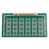
이 양면 FR4 TG170 PCB는 다재다능하고 비용 효율적인 솔루션입니다.. 산업 제어 시스템부터 가전제품, 의료 기기에 이르는 응용 분야에 적합합니다.. 1.6mm 두께로, 1오즈 구리 층, 무연 HAL 표면 마감, 이 PCB는 기계적 강도의 균형을 유지합니다., 전기 신뢰성, 및 환경 준수. 그러므로, 대규모로 일관된 성능을 요구하는 중간 수준의 복잡성을 지닌 전자 장치에 이상적입니다..
유리 전이 온도가 높은 FR4 소재로 제작 (tg) 170 ° C, 이 PCB는 향상된 열 안정성을 제공합니다.. 표준 FR4와 비교 (TG130 ° C), -20°C에서 +80°C 사이의 온도 변동이 있는 환경에서 더 나은 성능을 발휘합니다.. 이러한 장점은 안정적인 작동을 보장합니다.. 또한 양면 설계를 통해 엔지니어는 복잡한 회로를 효율적으로 라우팅할 수 있습니다.. 전원 및 접지면을 위한 이중 레이어 신호 트레이스와 구리 주입으로 전자기 간섭 감소 (에미) 신호 무결성을 향상시킵니다.. 결과적으로, 마이크로컨트롤러와 같은 중저속 애플리케이션을 지원합니다., 센서 인터페이스, 및 통신 모듈.
무연 hal 표면 마감: 이 마감재는 RoHS 및 REACH를 준수합니다.. 우수한 납땜성과 우수한 내식성을 제공합니다.. 추가적으로, 수동 및 자동 조립 모두에 적합합니다., 특히 빈번한 재작업이 필요한 애플리케이션의 경우.
1OZ 구리층: 두께 35μm, 구리 레이어는 넓은 트레이스당 최대 8A의 적당한 전류 부하를 지원합니다.. 최소 100μm/100μm의 라인/공간으로 미세한 라인 라우팅을 가능하게 합니다.. 이는 전력 공급과 높은 구성 요소 밀도의 균형을 유지합니다..
녹색 LPI 솔더 마스크: 솔더 마스크는 조립 및 재작업에 대한 시각적 명확성을 향상시킵니다.. 게다가, 오일과 같은 일반적인 산업 오염물질에 저항합니다., 용매, 그리고 청소제. 그러므로, 제조 공장이나 실외 장비와 같은 열악한 환경에 이상적입니다..
PCB는 품질과 신뢰성을 보장하기 위해 정밀하게 제작됩니다.:
±50μm 공차의 고정밀 기계식 드릴링으로 정확한 비아 보장.
도금된 관통 구멍 (PTH) 강력한 층간 연결을 위해 25-35μm 구리 코팅을 받음.
UV 리소그래피는 100μm 분해능으로 미세한 회로 패턴을 정의합니다..
주석 도금은 에칭 중에 전도성 흔적을 보호합니다.
내구성이 뛰어난 녹색 LPI 솔더 마스크는 150°C에서 경화됩니다..
100% 전기 테스트 (e- 테스트) 연속성과 격리성을 확인합니다..
자동화 된 광학 검사 (AOI) 솔더 마스크 커버리지 확인 및 결함 감지.
결함이 있는 패널은 엄격히 거부됩니다., 완벽한 PCB만 고객에게 배송되도록 보장.
산업 제어: PLC 모듈에 적합, 릴레이 제어 보드, 신뢰성과 경제성을 최우선으로 하는 센서 인터페이스.
소비자 전자 장치: 저전력 스마트 기기 지원, 웨어러블, 컴팩트한 디자인과 접근 가능한 테스트 포인트를 갖춘 오디오 모듈.
의료 기기: RoHS 준수, 안정적인 성능을 요구하는 진단 및 모니터링 장비에 적합합니다..
프로토 타이핑 & 교육: 표준 SMT/DIP 구성요소와의 호환성으로 인해 신속한 프로토타이핑에 인기가 높습니다..
IPC-6012 클래스 충족 2 산업용 애플리케이션 표준.
RoHS/REACH를 완벽하게 준수.
열 스트레스 테스트를 거쳤습니다. (260°C 리플로우) 그리고 진동 저항 (5-500HZ).
High-Tg 기질을 결합함으로써, 무연 hal 마감, 그리고 양면 디자인, 이 PCB는 신뢰할 수 있는, 확장 가능, 비용 효율적인 플랫폼. 산업을 발전시키는 엔지니어, 소비자, 또는 의료 전자 제품은 이 솔루션이 신뢰할 수 있고 글로벌 표준을 준수한다는 것을 알게 될 것입니다..