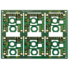
8-layer FR4 PCB is engineered for high-density electronic designs that require a balance of signal integrity, power distribution, and compact form factors, such as consumer electronics, medical devices, and industrial control modules. 그만큼 8-레이어 아키텍처 (typically 4 신호 레이어 + 4 전원/지상 비행기) enables complex routing for fine-pitch components while minimizing electromagnetic interference (에미). 그만큼 1.2mm board thickness offers a lightweight yet rigid foundation, ideal for space-constrained applications where weight and durability are critical.


Constructed with FR4 material, the PCB provides reliable electrical insulation (dielectric constant εr=4.5) and mechanical stability, suitable for a wide range of operating environments. 그만큼 2온스 (70μm) 구리 두께 on all layers enhances current-carrying capacity (추적 당 최대 15a) while maintaining design flexibility for both power and signal traces. 그만큼 Green LPI (Liquid Photoimageable) solder mask not only protects the circuitry from environmental damage but also improves visual inspection accuracy, 동안 흰색 실크 스크린 ensures clear component marking and designations for assembly and maintenance.


A key feature is the 동의하다 (전기 전기 니켈 몰입 금) surface treatment, which provides a smooth, corrosion-resistant finish for excellent solderability. The nickel layer (3–5μm) 내구성을 추가합니다, 그리고 금 층 (0.05–0.1mm) 산화를 방지합니다, making it suitable for long-term use. 그만큼 POFV (Plated Over Filled Vias) technology further enhances the PCB’s reliability: vias are filled with conductive material and plated over, eliminating voids that could cause thermal stress or solder wicking. This is particularly important for high-density designs with fine-pitch components (예를 들어, 0.5mm pitch BGAs) and ensures consistent performance in reflow soldering processes.


Manufacturing this PCB involves advanced techniques to ensure precision and quality:


  • Laser Direct Imaging (LDI) achieves fine-line accuracy (minimum line width/space: 50μm/50μm) for complex routing.
  • POFV processing uses conductive epoxy or resin to fill vias, followed by plating to create a smooth surface.
  • 100% AOI (자동화 된 광학 검사) verifies solder mask coverage and silkscreen clarity.
  • 전기 테스트 ensures continuity and isolation resistance, IPC-6012 수업 충족 2 표준.


Engineers will appreciate the PCB’s versatility in handling both high-density signal routing and moderate power applications. In consumer electronics, it supports compact designs for smartphones, 태블릿, and wearables, where space is at a premium. In medical devices, the POFV technology and ENIG finish contribute to long-term reliability in diagnostic equipment. In industrial systems, the 2OZ copper and FR4 material provide the durability needed for control panels and automation modules.


By choosing this 8-layer FR4 PCB with 2OZ copper, ENIG finish, and POFV technology, customers gain a solution that balances density, 신뢰할 수 있음, and cost-effectiveness. Its combination of advanced via filling, premium surface treatment, and precise manufacturing makes it a strategic choice for applications where component integration and long-term performance are essential. ISO에 의해 지원됩니다 9001:2015 certification, this PCB ensures consistent quality from prototyping to mass production.

PCB 기능


표준 PCB 맞춤형 PCB
레이어 수 2-20 2-50
재료 FR4 대만 연합의 고속 재료, 그리고 기술, Rogers 등의 고주파 재료.
PCB 두께 0.4-3.2mm 0.4-6.4mm
구리 중량 가져 오기 -3o 가져 오기 10
최소. 구멍 직경 0.3mm 0.1레이저 드릴에 의한 MM
PCB 크기 최소. 6.00x6.00mm 최대. 600.00x620.00mm
PCB 마감 할, Hal-Leadfree, 동의하다, Enepic, 침지 주석, 침수은, OSP
Min.Soldermask 댐. 41oz에 대한 MILS 2.51oz에 대한 MILS
Prepreg 유형 2116,1080 2116,1080,7628,3313,106
Min.Width/Space 4/4 밀스 2.5/2.5 밀스
최소. 환형 반지 4/4 밀스 2.5/2.5 밀스
종횡비 8:1 15:1
리드 타임 2 주 5 날 - 5 주
임피던스 공차 ±5% - ±10% ±5% - ±10%
다른 기술 금 손가락, 맹인과 묻힌 구멍, 껍질을 벗길 수있는 솔더 마스크, 가장자리 도금, 카본 마스크, 카운터 싱크 구멍,
반/카스텔 화 구멍, Fit Hole을 누릅니다, 수지로 꽂고 채워진 것을 통해, 패드를 통해 (요일, POFV), 하나의 PCB에서 다재다능합니다

이것은 닫힙니다 0

PCBA 기능


아니요. 프로세스 기능 매개 변수
1 주문 수량 1pc 이상
2 PCB 유형 강성 PCB, FPC, RIDID-FLEX PCB
3 어셈블리 기술 smt, tht, 혼합 기술 또는 팝
4 구성 요소 소싱 완전한 턴키, 부분적인 턴키, 위탁
5 PCB 크기 45*45mm -- 510*500mm
6 BGA 패키지 bga 그녀. 0.14mm, BGA 0.2mm 피치
7 부품 프레젠테이션 줄자, 릴, 스틱 또는 트레이
8 철사 & 케이블 와이어 하네스 및 케이블 어셈블리
9 품질 검사 시각적, SPI, FAI, AOI; 엑스선 점검
10 장착 정확도 ±0.035mm (±0.025mm)
11 최소 패키지 01005 (0.4mm*0.2mm)
12 적합성 코팅 머신에서 사용할 수 있습니다
13 IC 검사 기능, 전기 또는 삭제 테스트
14 리드 타임 3 날 - 5 주
15 다른 기술 박스 빌드 어셈블리, IC 프로그래밍, 구성 요소 비용 다운, 기능 & 노화 테스트 커스텀으로서,
Fit Assembly를 누릅니다, SAC305 또는 더 나은 솔더 페이스트 사용, BGA realling 또는 재 작업,
EMI 방출 제어를위한 방패 덮개 어셈블리

이것은 닫힙니다 0

FPC 기능


아니요. 프로세스 기능 매개 변수
1 레이어 수 1-8 레이어
2 FPC 자료 pi, 애완 동물, 펜, FR-4
3 최종 두께 0.06-4.0mm
4 보드 크기 250.00x1200mm
5 구리 호일 12하나,18하나,35하나,70하나
6 최소 폭/공간 3천/3mil
7 홀로 볼 구리 두께 8-20μm
8 표면 처리 홀 리드 드리, 동의하다, 몰입은/주석, OSP
9 차원을 개요합니다 ± 2mil
10 솔더 내열 저항 280℃ / 10SECS
11 보강재 유형 pi, FR4, 스테인레스 스틸, 알류미늄
12 최소. 홀 데이 (PTH) 0.1mm ± 3mils
13 최소. 홀 데이 (npth) 0.25± 2mil
14 최대/최소 솔더 마스크 두께 2MIL/0.5mil (501/12.7um)
15 최소 슬롯 0.8mm × 1mm

이것은 닫힙니다 0