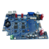
This 2-layer FR4 PCBA (Printed Circuit Board Assembly) is engineered for miniature electronic devices that demand a balance of reliability, conductivity, and assembly precision, such as wireless modules, wearable electronics, and medical sensors. With dimensions of 40mm×25mm and a 1.6MM 두께, the board maximizes space efficiency while supporting dense surface-mount component placement. 건축 FR4 material, it offers consistent electrical insulation and mechanical stability, suitable for commercial-grade applications with moderate temperature and humidity ranges.


그만큼 1온스 (35μm) 구리 두께 on both layers optimizes signal integrity and current-carrying capacity (넓은 흔적 당 최대 8A), ideal for battery-powered devices. 그만큼 Red LPI solder mask provides a durable, moisture-resistant coating that protects circuitry while enabling visual differentiation in multi-board assemblies, 동안 흰색 실크 스크린 ensures clear component marking for quality control and maintenance. 그만큼 동의하다 (전기 전기 니켈 몰입 금) surface finish creates a corrosion-resistant, solder-friendly surface (3–5μm nickel, 0.05–0.1μm gold), ensuring reliable connections for fine-pitch components (down to 0.3mm pitch).

SMT Assembly Capabilities

  • Component Support:
    • 01005 에게 1206 passive components
    • QFP, BGA (0.5mm pitch), 그리고 0201 ultra-small packages
    • Height restriction: ≤5mm for vertical clearance
  • Assembly Processes:
    • Lead-free reflow soldering (peak temperature: 260°C)
    • Automated optical inspection (AOI) for solder joint quality
    • X-ray inspection for BGA/CSP components
  • Testing Options:
    • In-circuit testing (ICT) for component functionality
    • 기능 테스트 (FT) per customer specifications

4×5 Panel Format Advantages

  • Production Efficiency:
    • 20 identical boards per panel reduce material waste by 30%
    • Breakaway tabs with V-cut scoring for easy depaneling
  • Cost Optimization:
    • Economies of scale for high-volume orders (10k+ units)
    • Shared setup costs across panels
  • Assembly Compatibility:
    • Compatible with standard pick-and-place machines (예를 들어, Yamaha, Juki)
    • Supports tape-and-reel component feeding

품질 관리 & 규정 준수

  • Material Traceability:
    • RoHS-compliant components (lead-free, halogen-free)
    • UL 94V-0 flammability rating for FR4
  • Reliability Testing:
    • Thermal cycling (-40°C to +85°C, 100 cycles)
    • Humidity testing (85°C/85% RH, 1,000 hours)
  • 표준이 충족되었습니다:
    • IPC-A-610 Class 2 for general electronics
    • ISO 9001:2015 quality management system

응용 프로그램

  • Wireless Communication:
    Bluetooth/Wi-Fi modules for IoT gateways and smart home devices
  • Medical Diagnostics:
    Portable health monitors with compact sensor interfaces
  • 소비자 전자 장치:
    Wearable fitness trackers and hearables with space-constrained designs
  • Industrial Sensors:
    Compact environmental sensors for predictive maintenance


By choosing this 2-layer FR4 PCBA, engineers gain a fully assembled solution that balances precision SMT placement, ENIG reliability, and panelized production. The red solder mask offers visual differentiation in complex systems, while the 4×5 panel format ensures cost-effective scaling from prototype to mass production. Backed by comprehensive testing and compliance, this PCBA delivers consistent performance for applications where size, 비용, and quality are critical.

PCB 기능


표준 PCB 맞춤형 PCB
레이어 수 2-20 2-50
재료 FR4 대만 연합의 고속 재료, 그리고 기술, Rogers 등의 고주파 재료.
PCB 두께 0.4-3.2mm 0.4-6.4mm
구리 중량 가져 오기 -3o 가져 오기 10
최소. 구멍 직경 0.3mm 0.1레이저 드릴에 의한 MM
PCB 크기 최소. 6.00x6.00mm 최대. 600.00x620.00mm
PCB 마감 할, Hal-Leadfree, 동의하다, Enepic, 침지 주석, 침수은, OSP
Min.Soldermask 댐. 41oz에 대한 MILS 2.51oz에 대한 MILS
Prepreg 유형 2116,1080 2116,1080,7628,3313,106
Min.Width/Space 4/4 밀스 2.5/2.5 밀스
최소. 환형 반지 4/4 밀스 2.5/2.5 밀스
종횡비 8:1 15:1
리드 타임 2 주 5 날 - 5 주
임피던스 공차 ±5% - ±10% ±5% - ±10%
다른 기술 금 손가락, 맹인과 묻힌 구멍, 껍질을 벗길 수있는 솔더 마스크, 가장자리 도금, 카본 마스크, 카운터 싱크 구멍,
반/카스텔 화 구멍, Fit Hole을 누릅니다, 수지로 꽂고 채워진 것을 통해, 패드를 통해 (요일, POFV), 하나의 PCB에서 다재다능합니다

이것은 닫힙니다 0

PCBA 기능


아니요. 프로세스 기능 매개 변수
1 주문 수량 1pc 이상
2 PCB 유형 강성 PCB, FPC, RIDID-FLEX PCB
3 어셈블리 기술 smt, tht, 혼합 기술 또는 팝
4 구성 요소 소싱 완전한 턴키, 부분적인 턴키, 위탁
5 PCB 크기 45*45mm -- 510*500mm
6 BGA 패키지 bga 그녀. 0.14mm, BGA 0.2mm 피치
7 부품 프레젠테이션 줄자, 릴, 스틱 또는 트레이
8 철사 & 케이블 와이어 하네스 및 케이블 어셈블리
9 품질 검사 시각적, SPI, FAI, AOI; 엑스선 점검
10 장착 정확도 ±0.035mm (±0.025mm)
11 최소 패키지 01005 (0.4mm*0.2mm)
12 적합성 코팅 머신에서 사용할 수 있습니다
13 IC 검사 기능, 전기 또는 삭제 테스트
14 리드 타임 3 날 - 5 주
15 다른 기술 박스 빌드 어셈블리, IC 프로그래밍, 구성 요소 비용 다운, 기능 & 노화 테스트 커스텀으로서,
Fit Assembly를 누릅니다, SAC305 또는 더 나은 솔더 페이스트 사용, BGA realling 또는 재 작업,
EMI 방출 제어를위한 방패 덮개 어셈블리

이것은 닫힙니다 0

FPC 기능


아니요. 프로세스 기능 매개 변수
1 레이어 수 1-8 레이어
2 FPC 자료 pi, 애완 동물, 펜, FR-4
3 최종 두께 0.06-4.0mm
4 보드 크기 250.00x1200mm
5 구리 호일 12하나,18하나,35하나,70하나
6 최소 폭/공간 3천/3mil
7 홀로 볼 구리 두께 8-20μm
8 표면 처리 홀 리드 드리, 동의하다, 몰입은/주석, OSP
9 차원을 개요합니다 ± 2mil
10 솔더 내열 저항 280℃ / 10SECS
11 보강재 유형 pi, FR4, 스테인레스 스틸, 알류미늄
12 최소. 홀 데이 (PTH) 0.1mm ± 3mils
13 최소. 홀 데이 (npth) 0.25± 2mil
14 최대/최소 솔더 마스크 두께 2MIL/0.5mil (501/12.7um)
15 최소 슬롯 0.8mm × 1mm

이것은 닫힙니다 0