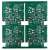
이 컴팩트한 2레이어 FR4 PCB는 신뢰성의 균형을 요구하는 소형 전자 장치용으로 설계되었습니다., 전도도, 그리고 비용 효율성, 웨어러블 기술과 같은, IoT 센서, 의료 진단. 치수와 함께 15.60mm×6.40mm 그리고 a 1.0MM 두께, 보드는 표면 실장 부품 조립을 위한 기계적 안정성을 유지하면서 공간 효율성을 극대화합니다.. 건축 FR4 재료, 일관된 전기 절연을 제공합니다. (유전 상수 εR = 4.5) 상용 등급 응용 분야에 적합한 내열성 및 내열성.
그만큼 1.5온스 (52μm) 구리 두께 두 레이어 모두에서 전류 전달 용량을 최적화합니다. (넓은 트레이스당 최대 10A) 보드 무게를 최소화하면서 전력 밀도와 수명이 중요한 배터리 구동 장치에 이상적입니다.. 그만큼 블루 LPI (액체 사진 이미지 가능) 솔더 마스크 내구성을 제공합니다, 환경적 손상으로부터 회로를 보호하는 방습 코팅, 동안 흰색 실크 스크린 소형 표면에 명확한 구성요소 마킹을 보장합니다., 좁은 레이아웃에서 조립 및 유지 관리 지원. 그만큼 출혈 (열풍 솔더 레벨링) 표면 마감이 균일함을 만듭니다., 공융 주석-납의 납땜 친화적 코팅 (또는 무연 SAC 합금), 미세한 피치 부품에도 안정적인 납땜 촉진 (0.5mm 피치까지).
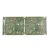
다음에서 제조됨 10×10 패널 형식, PCB는 재료 낭비를 최소화하고 픽 앤 플레이스 조립을 간소화하여 비용 효율적인 대량 생산을 가능하게 합니다.. 각 패널에는 다음이 포함됩니다. 100 동일한 보드, 섬세한 회로를 손상시키지 않고 패널을 쉽게 분리할 수 있도록 마이크로 비아 또는 분리 탭으로 연결됨. 이 형식은 소형 장치의 대량 생산이 필요한 OEM에 이상적입니다., 무선 모듈이나 센서 노드 등.
- 정밀한 라우팅:
- 최소 선 너비/공간: 60μm/60μm, 레이저 직접 이미징을 통해 달성 (LDI) 정확한 추적 정의를 위해.
- HASL 공정 제어:
- 무연 SAC305 합금 (96.5Sn/3.0Ag/0.5Cu) 몰입시간과 함께 <5 구리 산화를 방지하는 초.
- 품질 보증:
- 100% AOI (자동화 된 광학 검사) 솔더 마스크 적용 범위 및 실크스크린 정확도.
- 전기 연속성을위한 비행 프로브 테스트, 보장 <0.1모든 트레이스의 Ω 저항.
- 열 안정성:
- 최대 260°C의 리플로우 온도를 견딤 (무연 공정), 열 순환 테스트를 통해 검증됨 (-40°C ~ +85°C 1,000 사이클).
- 웨어러블 전자제품:
피트니스 트래커 강화, 스마트워치, 소형 회로와 로우 프로파일 디자인을 갖춘 건강 모니터.
- IoT 센서:
배터리 구동 환경 센서 활성화 (온도, 습기, 공기질) 스마트 빌딩이나 농업용.
- 의료 기기:
소형 진단 도구 또는 웨어러블 환자 모니터 지원, 크기와 신뢰성이 중요한 곳.
- 무선 모듈:
Bluetooth용 RF 회로 내장, Wi-Fi, 또는 가전제품 및 산업 자동화 분야의 Zigbee 모듈.
이 2층 FR4 PCB를 선택함으로써, 엔지니어는 1.5OZ 구리 성능의 균형을 맞추는 소형 솔루션을 얻습니다., 블루 솔더 마스크 내구성, 및 HASL 납땜성. 10×10 패널 형식은 프로토타입부터 대량 생산까지 비용 효율적인 확장을 보장합니다., 컴팩트한 크기로 인해 가장 작은 전자 장치에 통합될 수 있습니다.. ISO에 의해 지원됩니다 9001:2015 인증 및 IPC-6012 클래스 2 규정 준수, 이 PCB는 공간이 필요한 응용 분야에 일관된 품질을 제공합니다., 비용, 신뢰성은 타협할 수 없습니다.

")