

PCB에서, 언뜻 보기에는 중요하지 않은 것처럼 보이지만 실제로는 "특별한 표시"가 있습니다., 사실은, 설계부터 제조까지 원활한 작업 흐름을 보장하는 데 중요, 테스트, 그리고 최종 배송. 그 중, 테스트 지점과 구멍 찾기는 제품 기능과 생산 효율성을 보호하는 "보이지 않는 영웅" 역할을 합니다..
잘못 설계된 테스트 포인트로 인해 디버깅 주기가 길어진 적이 있습니까?? 또는 부정확한 구멍 위치 지정으로 인해 SMT 수율이 감소합니다.? 이 기사에서는 테스트 포인트의 중요한 역할을 보여줍니다., 구멍 찾기, 및 기타 특수 식별자 PCB—전체 PCB 수명주기에 걸쳐 그 가치를 설명합니다..
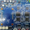
1. PCB 테스트 포인트: 기능성과 신뢰성의 생명선
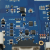
PCB 테스트 포인트 (테스트 포인트) PCB 제조 중 전기 테스트를 위해 예약된 전도성 영역입니다., 집회, 그리고 디버깅. 일반적으로 노출된 패드로 나타납니다., 비아, 또는 특별히 설계된 프로브 포인트, 자동화된 테스트 장비 간의 가교 역할 (ICT와 같은 - 회로 내 테스트 🔎) 그리고 보드의 회로.
기능 및 유형:
-
ICT (회로 내 테스트): 단락과 같은 일반적인 제조 결함을 감지하는 데 사용됩니다., 열립니다, 또는 구성 요소가 잘못 배치되었거나 누락되었습니다.. 테스트 포인트를 통해 ICT 시스템은 신속하게 결함을 찾을 수 있습니다., 생산 효율성 및 수율 향상.
-
FCT (기능 테스트): 테스트 포인트는 기능 테스트를 위한 액세스 포인트 역할을 합니다., 실제 작동을 시뮬레이션하여 전체 PCB 성능을 검증합니다..
-
디버깅 & 수리하다: 제품 개발 또는 판매 후 유지 관리 중, 엔지니어는 신호 측정 및 결함 진단을 위해 테스트 포인트에 의존합니다..
테스트 포인트의 종류:
-
패드형 테스트 포인트: 테스트를 위해 기존 구성 요소 패드 또는 전용 패드 사용.
-
비아 유형 테스트 포인트: 스루홀 또는 블라인드 비아를 테스트 지점으로 사용, 고밀도 PCB에서 자주 볼 수 있음.
-
프로브 패드: 스프링 프로브 접점용으로 설계된 특수 영역.
📢 디자인 고려 사항: 테스트 포인트 크기, 간격, 놓기, 적용 범위는 테스트 효율성에 직접적인 영향을 미칩니다.. 예를 들어, 테스트 포인트가 구성요소에 의해 차단되어서는 안 됩니다., 간격은 프로브 요구 사항을 충족해야 합니다. (일반적으로 ≥50mil), 주요 신호 경로와 전원/접지망을 포함해야 합니다.. 최적화된 레이아웃은 디버깅 및 문제 해결 시간을 최대로 단축할 수 있습니다. 30%.

2. PCB 위치 지정 구멍 및 기준점: 정밀 제조의 눈
위치 구멍 및 기준 표시는 자동화된 생산 및 조립 중 정밀한 정렬에 사용되는 특수 PCB 기능입니다.. 여러 프로세스에서 정확성을 보장합니다., 드릴링부터 SMT 배치까지.
기능 및 유형:
-
SMT 배치: 자동 픽 앤 플레이스 기계는 방향과 정렬을 위해 위치 구멍이나 기준점을 사용합니다., 정확한 부품 배치 보장.
-
교련 & 프로파일링: 구멍 가이드 드릴링 및 라우팅 기계 찾기, 보드 치수와 구멍 위치가 설계 사양과 일치하도록 보장.
-
테스트 픽스처 정렬: ICT/FCT 테스트 픽스처는 또한 위치 지정 구멍을 사용하여 정확한 프로브-테스트 지점 정렬을 보장합니다..
일반적인 유형:
-
공구 구멍: 보드 가장자리 또는 지정된 영역의 비도금 구멍, 제조 및 조립 전반에 걸쳐 기계적 정렬에 사용됩니다.. 일반적으로 오리엔테이션을 위해 쌍으로 또는 세 명씩 그룹으로 배치됩니다..
-
기준점: 노출된 구리 패드 (또는 솔더 마스크 개구부) 광학 인식을 위해 SMT 비전 시스템에서 사용됨. 글로벌 기준은 전체 보드를 정렬합니다., 로컬 기준점은 QFP 및 BGA와 같은 미세 피치 구성 요소를 정렬하는 데 도움이 됩니다..
🔎 정확도 요구 사항: 구멍 직경의 공차, 구멍 위치, 기준 모양/대비는 인식 정밀도에 직접적인 영향을 미칩니다.. 기준점은 일반적으로 직경이 1~3mm이고 솔더 마스크 간격이 명확하게 정의되어 있습니다., 높은 가시성 확보.

3. 기타 특수 표시: 통신 및 추적성 브리지
테스트 포인트를 넘어 구멍 찾기, PCB에는 제품 수명 주기 전반에 걸쳐 통신 및 추적성을 지원하는 다른 표시가 있습니다..
-
실크스크린 표시:
-
구성요소 지정자 & 극성 표시: 조립 및 수리 오류 방지.
-
회사 로고 & 제품 모델: 브랜딩 및 제품 식별용.
-
버전 번호 & 날짜 코드: 추적 및 개정 관리용.
-
-
원산지 표시: PCB의 제로 기준점 또는 방향을 나타냅니다..
-
솔더 마스크 개구부: 때때로 열 방출을 위해 사용됨, 접지, 또는 특별한 조립 요구 사항.
-
임피던스 제어 표시기: 중요한 임피던스 제어 트레이스를 보여주는 표시, 생산 검증 지원.
-
스택업 정보: 복잡한 다층 기판에는 제조 참조를 위한 단순화된 스택업 다이어그램이 포함될 수 있습니다..
📢 이러한 표시는 단순한 보드의 기호 그 이상입니다. 이는 디자인 간의 보편적인 "소통 언어" 역할을 합니다., 조작, 테스트, 집회, 그리고 수리하다. 생산 효율성을 향상시킵니다., 오류를 줄이다, 추적성을 보장합니다. 이를 무시하면 비용이 많이 드는 재작업이 발생할 수 있습니다., 지연, 또는 배치 수준의 품질 실패.

왜 선택해야 할까요? [완전 홍]: 원스톱 PCB/PCBA 파트너
~에 [완전 홍], 우리는 모든 것의 중요한 가치를 인식합니다. PCB 마킹. 우리의 전문 팀은 심층적인 설계 전문 지식과 광범위한 제조 및 테스트 경험을 결합합니다., 제품이 처음부터 품질과 효율성 모두에 최적화되도록 보장.
✅ DFM 우수성: 포괄적인 제조 적합성을 위한 설계 분석으로 테스트 포인트 보장, 구멍 찾기, 기준점은 IPC 표준 및 자동화된 생산 요구 사항을 완벽하게 준수합니다..
✅ 고급 테스트: 자체 ICT/FCT 장비와 엄격한 QC 프로세스를 통해, 전기적, 기능적 신뢰성을 보장하기 위해 테스트 포인트의 유용성을 극대화합니다..
✅ 정밀 제조: 고정밀 장비는 구멍 위치 결정을 보장하고 기준점은 탁월한 정밀도로 처리됩니다., 뛰어난 SMT 수율 제공.
✅ 엔드투엔드 솔루션: PCB 설계 및 제작부터 부품 소싱까지, PCBA 조립, 그리고 테스트, [완전 홍] 완벽한 원스톱 서비스를 제공하여 시간을 절약해 드립니다., 비용, 그리고 노력.
행동 촉구
제품의 성공은 세부 사항에 대한 관심에 달려 있습니다. 연락하다 [완전 홍] 오늘은 정밀 PCB 설계 및 제조 솔루션이 어떻게 제품 신뢰성과 시장 경쟁력을 향상시킬 수 있는지 알아보겠습니다.!


답장을 남겨주세요