오늘날 빠르게 변화하는 전자제품 세계에서, 스마트 웨어러블부터 항공우주 시스템까지 거의 모든 혁신은 하나의 필수 기반에 의존합니다.: the printed circuit board (PCB). But behind this seemingly simple green board lies a highly sophisticated and globalized industrial ecosystem. Have you ever wondered how your product idea can efficiently travel from concept to mass production with reliability and speed?
Understanding the structure, evolution, and dynamics of the global PCB supply chain allows companies to better plan their projects, optimize supply chains, 그리고, most importantly, choose a trustworthy manufacturing partner. 이 기사에서는, we’ll explore the evolution of the PCB industry, analyze the global collaboration model, uncover future trends, and highlight how 완전 홍 serves as your strategic partner to drive innovation with seamless, full-stack PCB/PCBA services.
1. From Hand Wiring to Smart Manufacturing: The Evolution of the PCB Industry
PCB (인쇄 회로 기판) reflect the progression of the entire electronics industry. Originally, components were manually wired — a slow and unreliable process. In the 1940s, printed circuit technology emerged, ushering in the era of single-sided PCBs, which improved production efficiency and product consistency.
By the second half of the 20th century, demand for higher functionality and miniaturization gave rise to multilayer boards, HDI (High-Density Interconnect), flex PCBs, and rigid-flex PCBs — critical for applications like smartphones and wearables. As globalization accelerated, manufacturing shifted to Asia, shaping today’s complex and segmented global PCB supply chain.
2. Anatomy of the Global PCB Supply Chain
The PCB ecosystem involves multiple stages and specialized participants:
✔ Design & Pre-Engineering
-
회로도 설계: Engineers draft circuit diagrams based on product functions.
-
PCB 레이아웃 설계: Using EDA tools, designers convert schematics into physical layouts. 제조 가능성을위한 설계 (DFM) is critical at this stage.
✔ Base Materials & Raw Supply
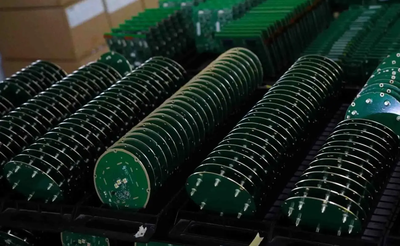
Includes copper-clad laminates (FR4, high-frequency, or flexible substrates), copper foils, solder masks, and plating chemicals — the quality of which directly impacts final product reliability.
✔ PCB Fabrication
-
이미징 & 에칭: Create circuit patterns by removing excess copper.
-
교련 & 도금: Ensure electrical connectivity through vias.
-
라미네이션: Combine multiple layers under heat and pressure.
-
솔더 마스크 & 실크 스크린: Protect circuits and print component labels.
-
표면 마감: Apply gold, OSP, or HASL for reliable solderability.
✔ Component Sourcing
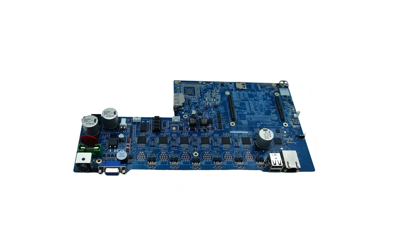
Procuring genuine, high-quality components (IC, 커넥터, 커패시터) from global suppliers is critical to avoid delays or defects — especially during shortages.
✔ PCBA Assembly
-
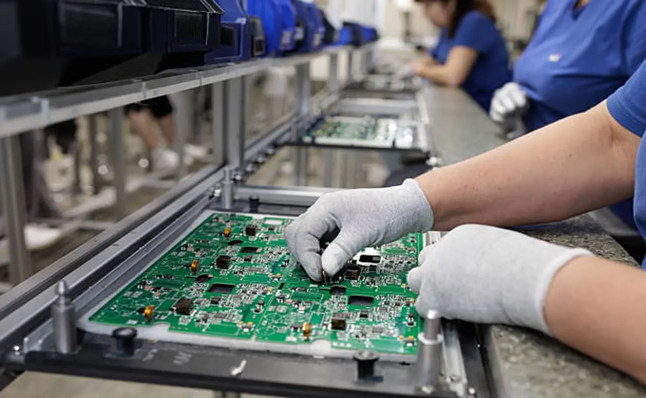
smt (표면 마운트 기술): High-speed placement of components followed by reflow soldering.
-
Wave/Selective Soldering: For through-hole components.
-
Manual Soldering: For custom or small-batch requirements.
✔ Testing & 점검
-
AOI (자동화 된 광학 검사)
-
X-Ray Inspection for hidden solder joints (BGA/QFN)
-
ICT (회로 테스트)
-
FCT (기능 테스트)
-
Aging Test under extreme conditions to ensure reliability.
3. Evolving Collaboration Models & Industry Challenges
As complexity grows, so does the need for specialization.
✦ Common Models:
-
EMS (전자제품 제조 서비스): Brands outsource production.
-
ODM (Original Design Manufacturer): Provides both design and manufacturing.
-
Turnkey One-Stop Services: Companies like Fully Hong handle everything from DFM, raw materials, 집회, 테스트, to global logistics — simplifying management and reducing time to market.
✦ Ongoing Challenges:
-
Supply Chain Resilience: Geopolitical tensions, chip shortages, and pandemic disruptions require adaptable planning.
-
Quality Traceability: Managing quality across multi-country supply networks is increasingly complex.
-
속도 & 사용자 정의: Rapid iteration and small-batch production demand flexible systems.
-
환경 준수: Sustainability is now a competitive advantage, not just a regulatory requirement.
4. What Drives Future PCB Development?
Technology Acceleration:
-
소형화 & Integration: HDI, SLP, and Embedded Components.
-
New Materials: For 5G, 일체 포함, EVs — low-loss, high-frequency substrates.
-
Function-Integrated Modules: SiP (System-in-Package) is blurring lines between PCB and semiconductor.
Market Expansion:
-
5G & 통신: Fueling demand for high-speed PCBs.
-
AIoT & 소비자 전자 장치: Requires low-power, high-reliability PCBA.
-
EVs & Automotive Systems: High-temperature and high-voltage PCBs.
-
의료 전자 장치: Micro PCBs for wearable diagnostics and implants.
Smart Manufacturing & Sustainability:
-
산업 4.0 Integration: Automation, predictive maintenance, and real-time analytics will drive efficiency.
-
Green Production: Lead-free, halogen-free materials, energy-efficient processes, and closed-loop recycling.
풀리홍을 선택하는 이유?
In a world of complexity and competition, Fully Hong is your one-stop partner for innovation, agility, and quality.
✅ Turnkey Services: From PCB layout, fabrication, global sourcing to precision PCBA and delivery — eliminate multi-vendor coordination.
✅ Global Sourcing Strength: We manage shortages, suggest reliable substitutes, and ensure stable supply with strategic reserves.
✅ Engineering & Quality Excellence: High-mix, high-density, or HDI — our expert team and world-class facilities ensure top-tier performance.
✅ Custom Solutions & 속도: Whether prototyping or scaling, we adapt to your needs with rapid response and personalized support.
📌 Let’s build the future, together. Don’t let fragmented supply chains slow you down. 파트너가 되어보세요 완전 홍 and turn your ideas into reality.
🌐 웹사이트: https://www.pcb-leader.com
📞 Mobile: +86 13798350430
📲 WeChat/WhatsApp: +86 13798350430 / +86 17722543446
📧 Email: info@lyly-hong.com
📠 Tel/Fax: +86-755-2664 8236


답장을 남겨주세요