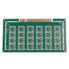
Ce PCB FR4 TG170 double face est une solution polyvalente et économique. Il convient aux applications allant des systèmes de contrôle industriels à l'électronique grand public et aux dispositifs médicaux.. D'une épaisseur de 1,6 mm, 1Couches de cuivre OZ, et une finition de surface HAL sans plomb, ce PCB équilibre la résistance mécanique, fiabilité électrique, et conformité environnementale. Donc, il est idéal pour l'électronique de complexité moyenne nécessitant des performances constantes à grande échelle.
Construit à partir d'un matériau FR4 avec une température de transition vitreuse élevée (Tg) de 170°C, ce PCB offre une stabilité thermique améliorée. Par rapport à la norme FR4 (Tg130°C), il fonctionne mieux dans des environnements présentant des fluctuations de température entre -20°C et +80°C. Cet avantage garantit un fonctionnement fiable. La conception double face permet également aux ingénieurs d'acheminer efficacement des circuits complexes. Les traces de signal à double couche et les coulées de cuivre pour les plans d'alimentation et de masse réduisent les interférences électromagnétiques. (EMI) et améliorer l'intégrité du signal. Par conséquent, il prend en charge les applications à vitesse faible à moyenne telles que les microcontrôleurs, interfaces de capteurs, et modules de communication.
Finition de surface HAL sans plomb: Cette finition est conforme RoHS et REACH. Il offre une excellente soudabilité et une bonne résistance à la corrosion. En plus, il convient aussi bien à l'assemblage manuel qu'automatisé, en particulier dans les applications nécessitant des retouches fréquentes.
1Couches de cuivre OZ: Avec une épaisseur de 35 μm, les couches de cuivre supportent des charges de courant modérées jusqu'à 8 A par large trace. Ils permettent un routage fin avec une ligne/espace minimum de 100 μm/100 μm. Cela équilibre la fourniture de puissance et la densité élevée des composants.
Masque de soudure LPI vert: Le masque de soudure améliore la clarté visuelle pour l'assemblage et la reprise. De plus, il résiste aux contaminants industriels courants comme les huiles, solvants, et produits de nettoyage. Donc, il est idéal pour les environnements difficiles tels que les usines de fabrication ou les équipements extérieurs.
Le PCB subit une fabrication précise pour garantir la qualité et la fiabilité:
Un perçage mécanique de haute précision avec une tolérance de ± 50 μm garantit des vias précis.
Trous traversants plaqués (Pth) recevez un revêtement de cuivre de 25 à 35 μm pour des connexions intercouches solides.
La lithographie UV définit des motifs de circuits fins avec une résolution de 100 μm.
L'étamage protège les traces conductrices pendant la gravure.
Le masque de soudure LPI vert durable durcit à 150 °C..
100% tests électriques (Test e) vérifie la continuité et l'isolement.
Inspection optique automatisée (AOI) vérifie la couverture du masque de soudure et détecte les défauts.
Les panneaux défectueux sont strictement rejetés, garantir que seuls des PCB impeccables soient expédiés aux clients.
Contrôle industriel: Convient aux modules API, cartes de contrôle de relais, et interfaces de capteurs privilégiant la fiabilité et la rentabilité.
Électronique grand public: Prend en charge les appareils intelligents à faible consommation, appareils portables, et modules audio avec des conceptions compactes et des points de test accessibles.
Dispositifs médicaux: Conforme à RoHS, il s'adapte aux équipements de diagnostic et de surveillance nécessitant des performances stables.
Prototypage & Éducation: Populaire pour le prototypage rapide grâce à la compatibilité avec les composants SMT/DIP standard.
Conforme à la classe IPC-6012 2 normes pour applications industrielles.
Entièrement conforme RoHS/REACH.
Testé pour le stress thermique (260refusion °C) et résistance aux vibrations (5-500HZ).
En combinant un substrat à haute Tg, finition HAL sans plomb, et conception double face, ce PCB offre une fiabilité, évolutif, et plateforme rentable. Ingénieurs développant des activités industrielles, consommateur, ou l'électronique médicale trouvera cette solution fiable et conforme aux normes mondiales.