
1.What is Design for Manufacturing / Assembly (DFM/DFA)
Design for Manufacturing and Assembly (DFMA) combines two methodologies:
-
Design for Manufacturing (DFM)
-
Design for Assembly (DFA)
This integration enables efficient manufacturing and easy assembly of a product design with minimal labor cost. Using DFM/A, a company can prevent, detect, quantify, and eliminate waste and inefficiencies in product design.
Traditional vs. DFM/A Approach
DFM/A breaks from tradition. Instead of the traditional method—where design engineers hand off drawings to manufacturing—DFM/A fosters collaboration. Design and manufacturing engineers work together to develop manufacturing and assembly methods simultaneously with the design.
Though DFM and DFA have traditionally been defined separately, for effective DFMA application, they must work together to gain the greatest benefit.
In PCB production, DFM and DFA analysis techniques bridge the gap between design and manufacturing, especially with tools that control key parameters. The absence or insufficiency of DFM/DFA can increase the PCB cost by up to 20%. Early application—before the first prototype—can avoid unexpected problems and costs.
2. How to Implement DFM/DFA in General Product Design
When implementing DFM/DFA in product development, the following strategies are recommended:
2.1 Reduce Component Parts and Simplify Design
Evaluate each part’s function. Eliminate or combine parts where possible. This reduces hardware, assembly steps, and potential errors

2.2 Design for Ease of Fabrication
Choose standard materials, remove unnecessary features, and involve manufacturing teams in design reviews to optimize fabrication and avoid costly tooling.
2.3 Operate Within Process Capabilities & Avoid Tight Tolerances
Understand manufacturing limits and avoid excessive tolerances. Check for tolerance stack-up to ensure proper fit and reduce rework costs.
2.4 Utilize Common Parts and Materials
Standardizing components across products reduces inventory, learning curves, and design risks.
2.5 Mistake-Proof the Design (Poka Yoke)
Add features (like tabs or asymmetric shapes) to prevent incorrect assembly. Mark critical quality dimensions.
2.6 Ensure Proper Handling and Orientation
Design parts that are easy to grasp, symmetrical, and consistently aligned to simplify manual or automated assembly.
2.7 Design for Ease of Assembly
Use intuitive movement paths and minimize tool changes or reorientation. Prioritize tool accessibility and ergonomic assembly.
2.8 Reduce or Eliminate Flexible Parts and Connectors
Avoid fragile cables by integrating more durable, fixed interconnects where possible.
2.9 Use Efficient Fastening Methods
Minimize fastener variety. Use snap fits, adhesives, or standardized hardware to accelerate assembly and ease maintenance.
2.10 Adopt Modular Product Design
Modular design allows for better scalability, easy customization, simplified repair, and reduced complexity.
2.11 Design for Automation
Ensure compatibility with robotic or automated processes. Parts should self-locate, require minimal orientations, and fit standard fixtures.

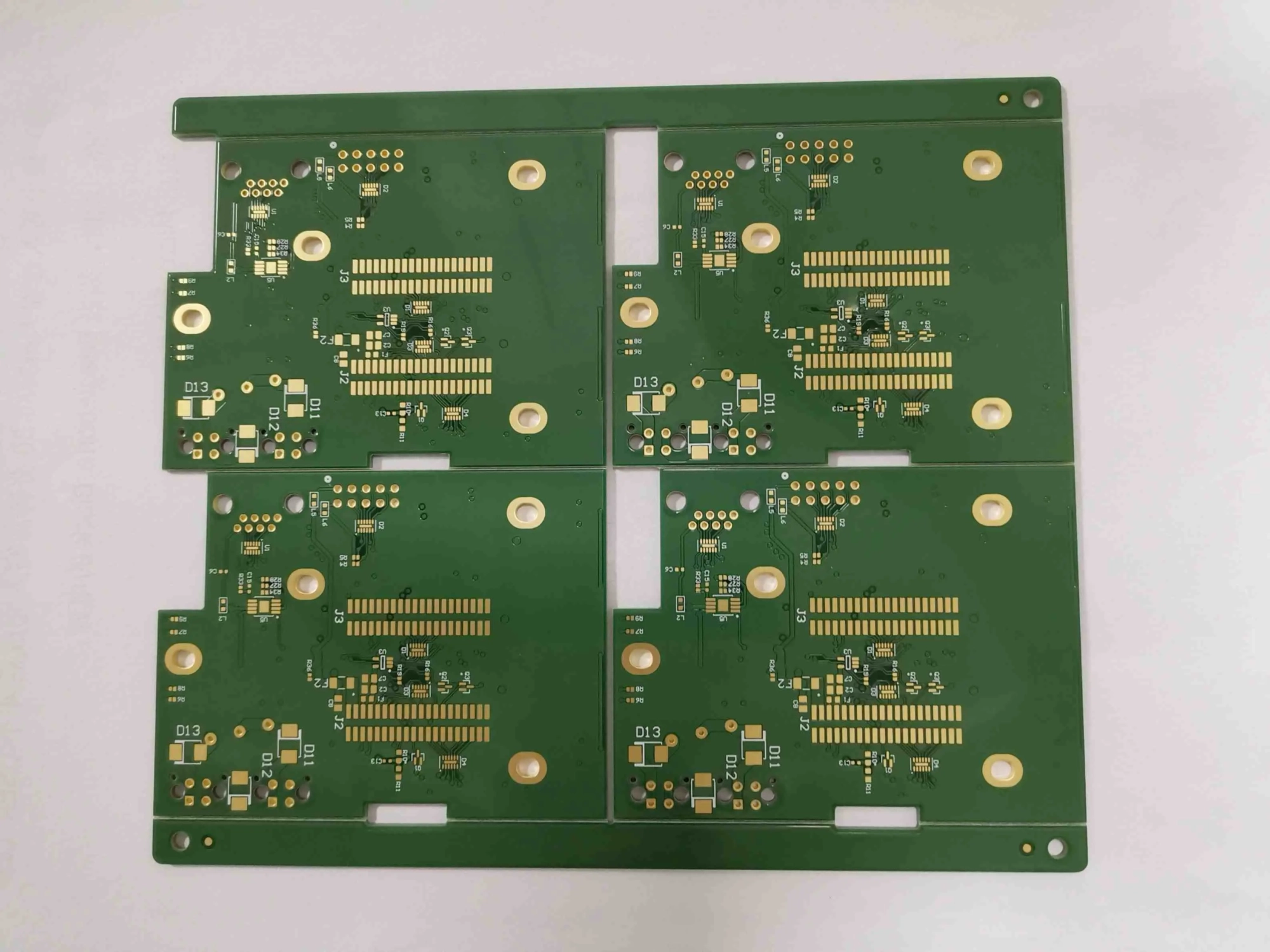
3. How to Perform DFM/DFA in PCB and PCBA Fields
3.1 Challenges in Modern PCB Design
As component sizes shrink and layout density increases, meeting design-for-manufacturing requirements becomes more complex. This is where DFM and DFA become essential.
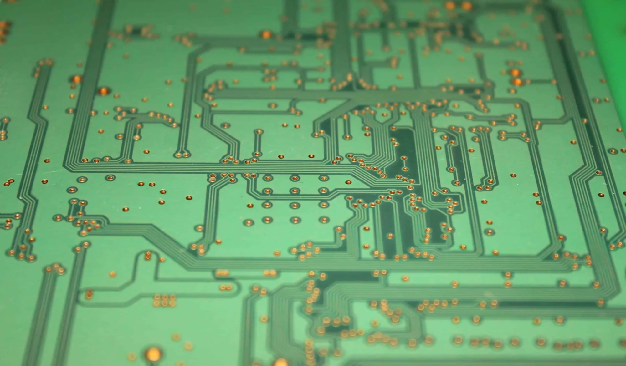
3.2 DFM in PCB Design
DFM ensures that the PCB layout complies with manufacturing standards, reducing errors before production.
Common DFM Problems & Solutions:
-
Acid Traps: Acute angles trap etching acid → Use arcs or 45° traces
-
Copper/Solder Mask Slivers: Thin fragments → Increase trace width, ensure proper spacing
-
Isolated Thermal Pads: Poor heat transfer → Connect pads efficiently
-
Insufficient Annular Rings: Risk of open circuits → Ensure adequate ring width
-
Copper Too Close to Edges: May cause short circuits → Maintain spacing
-
Improper Solder Mask: May expose traces → Apply solder mask precisely
-
Inappropriate Substrate: Leads to overheating → Choose material based on thermal and mechanical needs
3.3 DFA in PCB Design
DFA focuses on optimizing the design to facilitate cost-effective assembly.
Key DFA Considerations:
-
Component-Pad Match: Ensure alignment and footprint accuracy
-
Component Spacing: Prevent overcrowding, especially at board edges and during panelization
-
Solder Mask & Fiducials: Must be clear and present
-
Hole Sizes and Placement: Ensure correct positioning for component leads
-
Edge Clearance: Needed for handling and panel separation
-
Thermal Reliefs: Enable heat dissipation during soldering
-
Component Availability: Avoid obsolete or long-lead items
-
Panelization: Design boards for easy multi-board manufacturing
-
Testability: Include test points and clear access
-
Vibration Resistance: Ensure robustness under stress
Risks of Ignoring DFA:
-
Assembly delays
-
Rework and higher costs
-
Inconsistent quality and reliability issues

4. Conclusion
DFM and DFA are critical methodologies for both general product and PCB design. They help:
✅ Reduce design iterations
✅ Shorten time to market
✅ Lower defect rates
✅ Improve product reliability
✅ Cut production costs
By integrating DFM/DFA early in the development process, companies can enhance efficiency, profitability, and competitiveness in their markets.