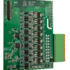
8-Layer PCB wurde für geschäftskritische industrielle Kommunikationsanwendungen entwickelt, wo Hochfrequenzsignalintegrität, elektromagnetische Verträglichkeit (EMC), und robuste Haltbarkeit sind unerlässlich. Mit Dimensionen von 190mm×170mm und a 1.7mm Dicke, Das Board vereint die Integration großflächiger Komponenten mit mechanischer Stabilität für industrielle Schaltschränke und Kommunikationshubs. Das Einzigartige Materialaufbau TU-862+RO4350B kombiniert die kostengünstige mechanische Festigkeit von TU-862 mit den verlustarmen dielektrischen Eigenschaften von RO4350B (Dk=3,48, tanδ=0,004 bei 10 GHz), Damit ist es ideal für die Hochgeschwindigkeits-Datenübertragung in Protokollen wie Ethernet, CANopen, und Profibus.
- Asymmetrische Kupferdicke:
- Äußere Schichten: 1Oz (35μm) für robuste Stromleiterbahnen und EMI-Abschirmung
- Innere Schichten: 0.5Oz (18μm) für die Signalführung mit feiner Tonhöhe
- Ermöglicht eine ausgewogene Stromverteilung (4 Kraft-/Bodenebenen) und Hochgeschwindigkeits-Signalschichten (4 Differentialpaarkanäle)
- Präzise Impedanzkontrolle:
- 50Ω ±8 % für Mikrostreifen-/Streifenleitungskonfigurationen
- Erreicht durch kontrollierte Berechnungen der dielektrischen Dicke und Leiterbahnbreite
- Minimiert die Signalreflexion in 10-Gbit/s-Ethernet- und industriellen drahtlosen Schnittstellen
- Nicht leitende gefüllte Vias (NCFV) mit Kupferkappe:
- Mit Harz gefüllte Durchkontaktierungen zur Vermeidung von Hohlräumen, Anschließend mit Kupfer überzogen, um eine glatte Oberfläche zu erzielen
- Eliminiert das Risiko einer Dochtwirkung von Lot in BGA-Bereichen und verbessert die Wärmeleitfähigkeit
- Sequentielle Laminierung:
- 8 Stufenweise laminierte Schichten, um eine gleichmäßige dielektrische Dicke und Registrierungsgenauigkeit zu gewährleisten (<50μm)
- Rätseloberfläche:
- 3-5μm-Nickelschicht für Korrosionsbeständigkeit
- 0.05-0.1μm-Goldschicht für langfristige Lötbarkeit
- Mattgrüne LPI-Lötmaske:
- Reduziert Blendung bei der AOI-Inspektion
- Bietet hervorragende chemische Beständigkeit in industriellen Umgebungen
- EMC/EMI -Minderung:
- In Abständen von 2 mm platzierte Groundplane-Stitching-Durchkontaktierungen zur Unterdrückung von Gleichtaktstörungen
- Präzises Differentialpaar-Routing mit präziser Längenanpassung 5 Mils (0.127mm) um einen minimalen Signalversatz zu gewährleisten
- Thermalmanagement:
- Thermische Durchkontaktierungen verbinden die Leistungsebenen mit den Außenschichten für eine effiziente Wärmeableitung
- Kupfergussbereiche auf Leistungsschichten, um Hotspots zu reduzieren
- Unterstützung für gemischte Baugruppen:
- SMT für ICs mit hoher Dichte (Z.B., PHY-Chips, FPGAs)
- DIP für robuste Steckverbinder (Z.B., RJ45, DB25) und Relais
- 100% Automatisierte Tests:
- Impedanzüberprüfung pro Schicht
- Röntgeninspektion von NCFV-Vias
- AOI für Lötstopplack- und Siebdruckqualität
- Umwelttests:
- Temperaturwechsel (-40° C bis +85 ° C., 1,000 Zyklen)
- Vibrationstests (5-500Hz, 2G Beschleunigung)
- Einhaltung von Standards:
- IPC-6012 Klasse 3 Für missionskritische Anwendungen
- RoHS/REACH für Gefahrstoffbeschränkungen
- IN 55032 Klasse A für elektromagnetische Emissionen
- Industrielle Ethernet-Switches:
Unterstützt 10GBASE-T und PoE+ mit minimaler Signalverschlechterung
- Drahtlose Basisstationen:
Ermöglicht 5G NR Sub-6GHz-Funkfrequenzrouting
- SPS & SCADA-Systeme:
Erleichtert den Echtzeit-Datenaustausch in Produktionsanlagen
- Eisenbahnkommunikationsnetze:
Trifft sich in 50155 Umweltstandards für Schienenfahrzeuganwendungen

")