
PCB Clone / PCB Reverse Engineering
What is PCB Reverse Engineering
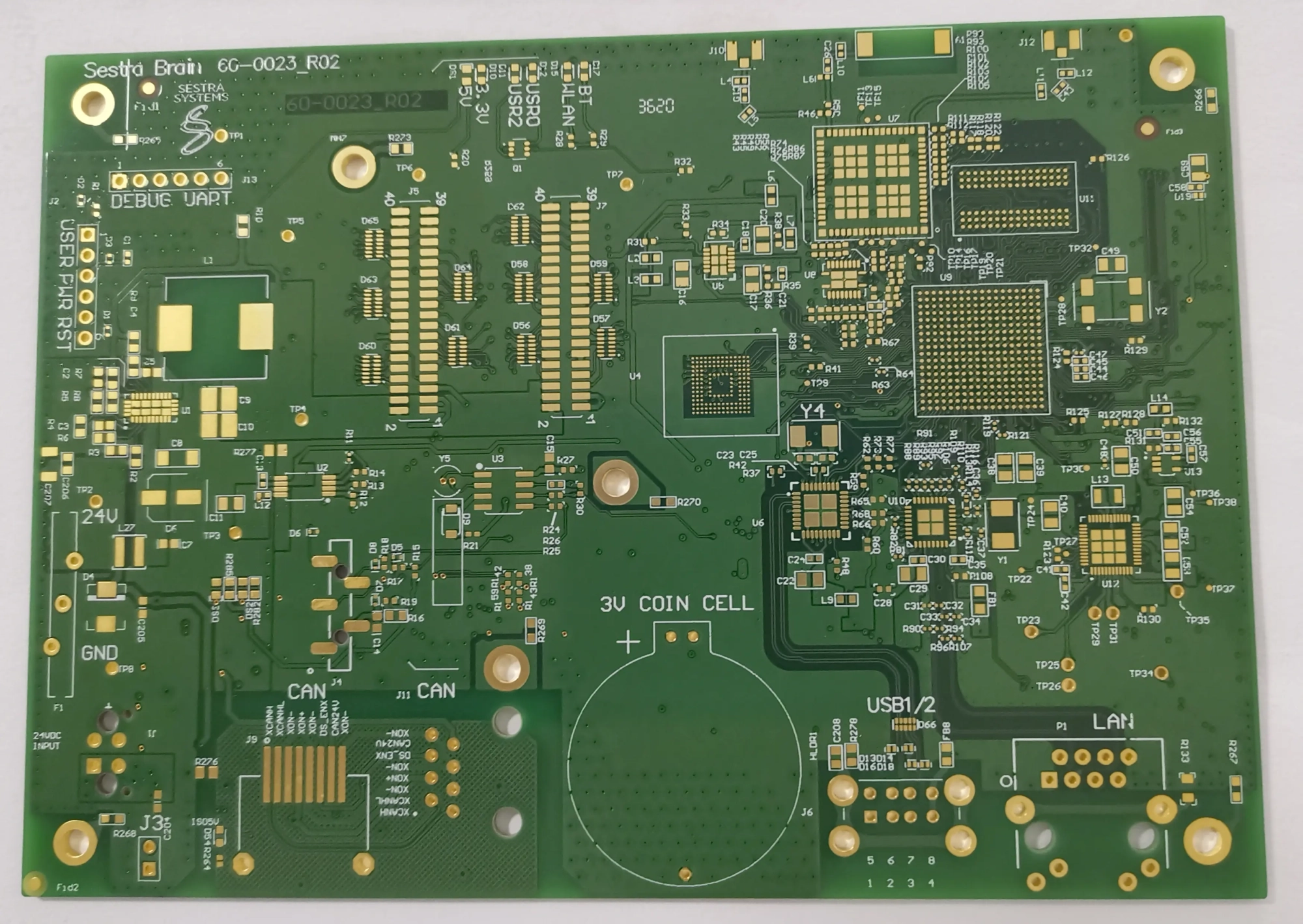
PCB reverse engineering (also known as PCB clone, PCB copy, PCB duplication, or PCB RE) is the process of analyzing an existing physical Printed Circuit Board (PCB) and recreating its design to produce a functionally identical copy.
This process includes several technical steps:
-
Extracting schematic diagrams
-
Generating Gerber files and PCB layout
-
Creating a Bill of Materials (BOM)
-
Using IC unlock technology to extract Bin or Hex code from programmable ICs
-
Reproducing the board through:
-
PCB fabrication
-
Component soldering
-
Flying probe testing
-
Circuit debugging
-
✅ The goal is to fully duplicate the original circuit board and ensure the same functionality.

What You Will Receive from Fully Hong Electronics
By choosing Fully Hong Electronics for your PCB reverse engineering or cloning project, you will receive:
📄 PCB Gerber Files
🧾 Complete BOM (Bill of Materials)
📐 Detailed Schematic Diagrams
🔧 Functional PCB Samples
What We Need from You
To initiate PCB or PCBA cloning, please prepare:
-
At least 2 physical samples of the PCB or PCBA
How to Clone a PCB / PCBA
1️⃣ Draw, Scan, or Photograph the PCB
-
Take clear photos of both sides of the board
-
Use a dark background to improve contrast (especially for boards with through-holes)
-
Use a high-resolution camera with sufficient lighting
-
Optionally, draw the layout on graph paper for simpler boards
2️⃣ Upload the Image
-
Crop the image to focus only on the PCB
-
Upload it to your reverse engineering software
-
Use photo editing tools to enhance visibility and highlight key features
3️⃣ Construct the PCB Layout
-
Use software (e.g., AutoTrace) to convert images to vector graphics
-
Build a 3D PCB layout to analyze electromagnetic behavior and circuit patterns
Editing Steps per Side:
-
Paint holes and solder pads
-
Remove PCB trackpads to avoid conversion loops
-
Mark unconnected holes
-
Adjust saturation and layers
-
Clean tracks and smooth edges
-
Convert to grayscale and invert for clear tracing
-
Repeat for both sides of the PCB

4️⃣ Create the Schematic Diagram
Once the layout is complete:
-
Generate 2D schematic drawings using CAD or layout software
-
Label each component and connection with standard symbols
-
Combine both sides of the board into a full schematic
Use this schematic to:
-
Troubleshoot
-
Modify
-
Repair
-
Reproduce the PCB
❓ Frequently Asked Questions (FAQs)
Q1: What is PCB reverse engineering?
PCB reverse engineering is the process of deconstructing and analyzing a printed circuit board to understand its design, components, and connections, typically for replication or improvement.
Q2: Why is PCB reverse engineering important?
It helps in replacing obsolete boards, understanding competitor designs, ensuring quality control, protecting IP, or customizing for specific use cases.
Q3: What are the main challenges?
-
Complex modern layouts
-
Access to inner layers
-
Component identification
-
Legal & ethical concerns
-
Accuracy of replication
Q4: What tools are typically used?
-
Optical & X-ray inspection
-
Multimeters, oscilloscopes, logic analyzers
-
CAD software for schematic and layout design
Q5: Best practices for PCB RE?
-
High-quality images and data
-
Systematic workflow
-
Use of professional tools
-
Documentation of each step
-
Legal compliance