
In today’s fast-paced electronics industry, transforming an innovative product concept into a reliable physical product is a challenging task. At the heart of this process lies Printed Circuit Board Assembly (PCBA). Even the most flawless designs can fail if minor defects occur during manufacturing, potentially leading to costly recalls and damaging brand reputation.
How can these risks be mitigated? The answer lies in a comprehensive and carefully designed testing strategy. Testing is not an optional step after production—it is a core process that ensures quality and controls costs throughout the manufacturing cycle. At fully-hong, we understand this principle deeply. We do more than assemble PCBs; we act as your quality partner, ensuring that every PCBA leaving our production line is precise and defect-free.
This article provides a detailed overview of the most widely used PCBA testing methods and helps you determine which strategy best fits your project.

First Line of Defense: Visual and Optical Inspection
Before electrical testing, it’s essential to verify that the PCB’s appearance meets standards.
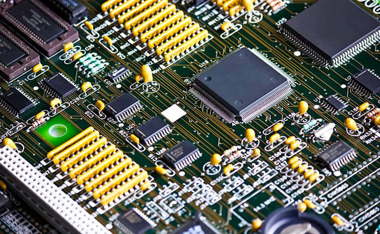
1. Automated Optical Inspection (AOI)
What is it? AOI is the “eagle eye” of modern PCBA production lines. High-resolution cameras capture images of the PCB, which are then compared to predefined standards to detect surface defects faster and more accurately than human inspection.
What can it detect? Missing components, misalignment, polarity errors, excessive or insufficient solder, and solder bridges.
Best for: Almost all mass-production workflows. As the first step in quality control, AOI detects issues early, enabling corrective action and preventing large-scale defects, maximizing cost efficiency.
Limitations: AOI only inspects visible surfaces and cannot detect hidden solder joints on components such as BGAs or QFNs.

Core Verification: Electrical and Connectivity Testing
Once the visual inspection is cleared, it’s crucial to ensure the electrical performance of the PCB meets design specifications.
2. In-Circuit Test (ICT)
What is it? ICT is one of the most comprehensive electrical testing methods. Custom “bed-of-nails” fixtures are designed to contact each test point on the PCB, measuring each component’s electrical characteristics individually.
What can it detect? Open circuits, short circuits, incorrect resistor/capacitor values, diode/transistor polarity errors, with coverage up to 98%.
Best for: Mature designs with high production volumes. For tens of thousands of units per year, the upfront fixture cost is offset by low per-unit testing costs and high efficiency.
Limitations: Fixtures are expensive, and design changes may require new fixtures, making ICT less suitable for prototypes or low-volume projects.
3. Flying Probe Test (FPT)
What is it? FPT is a flexible alternative to ICT. It uses 2–6 high-speed probes to contact pads or vias according to programmed instructions, without the need for custom fixtures.
What can it detect? Similar issues as ICT, including open circuits, short circuits, and component value/direction errors.
Best for: Prototype validation, low-volume production, and projects with diverse product types. FPT is highly flexible, and design changes only require program adjustments, with minimal startup costs.
Limitations: Testing speed is slower than ICT, making it less suitable for large-scale production.

“X-ray” Inspection: Advanced Non-Destructive Testing
4. Automated X-ray Inspection (AXI)
What is it? When AOI cannot see beneath components, AXI comes into play. X-rays penetrate the chip and PCB, providing clear images of hidden solder joints under BGA, LGA, or other high-density packages.
What can it detect? Voids, solder bridges, insufficient solder, and internal joint integrity issues.
Best for: High-reliability products with hidden-bottom components, such as communication, medical, and aerospace equipment.
Limitations: AXI is costly and slower and requires experienced operators to interpret results.

5. Functional Test (FCT)
What is it? FCT is the final checkpoint in the production process, simulating real-world usage conditions. The PCBA is powered on, and specific input signals are applied to verify whether outputs meet design specifications—essentially, “turn it on and see if it works.”
What can it detect? Overall functionality, interface signals, power consumption, and other system-level issues.
Best for: All products. FCT can be tailored from simple continuity checks to complex diagnostic routines, capturing potential problems other tests might miss.

6. Burn-in Test
What is it? Burn-in testing subjects PCBA to extreme conditions such as high temperature and voltage for extended periods to identify early-life failures.
What can it detect? Components prone to early failure under stress.
Best for: Products with high reliability requirements, including servers, medical devices, and automotive electronics.
Choosing the Right Testing Combination
No single test is sufficient for all scenarios. A successful project often requires a combination of methods:
-
Product stage: Flying Probe Test (FPT) is ideal for prototypes and low-volume production, while ICT excels in mass production.
-
PCB complexity: Designs with BGA/QFN require AXI.
-
Application field: Consumer electronics may prioritize AOI + FCT for cost-quality balance, whereas medical, industrial, or aerospace products may require AOI + AXI + ICT + FCT + Burn-in for zero-failure reliability.
-
Budget considerations: Our experts work with you to design a cost-effective testing strategy with maximum coverage.
Conclusion: Testing is an Investment, Not a Cost
Choosing a supplier that only knows manufacturing can lead to high risks and hidden costs. Partnering with fully-hong, which integrates comprehensive testing strategies into every stage, ensures quality assurance throughout your project lifecycle.
We believe rigorous testing is the only path to exceptional products.
Are you ready to build a solid quality foundation for your next PCBA project?


Leave a reply