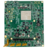
8-Layer FR4 PCB: The Core Board for Industrial Communication
This 8-layer FR4 PCB is specifically engineered for demanding industrial communication applications, providing a stable and reliable foundation for industrial control cabinets, communication gateways, and automation systems. With dimensions of 174.52×121.25mm and a thickness of 1.6mm, the board balances mechanical stability with the ability to integrate a large number of critical components. From excellent signal integrity to a durable build, this PCB is designed to deliver reliable performance in harsh environments with vibration, temperature fluctuations, and electromagnetic interference.
Key Technical Features
1. Advanced Stackup and Signal Integrity
- 8-Layer Stackup: The design features four signal layers and four power/ground planes. This architecture effectively suppresses EMI (Electromagnetic Interference) and provides optimized routing paths for high-speed differential pairs like Ethernet and CANopen.
- Precision Impedance Control: Differential line impedance is controlled at 100Ω±8%, while single-ended line impedance is controlled at 50Ω±8%. This minimizes signal reflection and ensures the integrity of high-speed interfaces like Gigabit Ethernet.
- 1OZ (35μm) Copper Thickness: The copper thickness balances the needs of fine-line routing (minimum line/space: 75μm/75μm) with a high current-carrying capacity of up to 10A, supporting high-power and high-density designs.
2. Industrial-Grade Design and Manufacturing
- ENIG (Electroless Nickel Immersion Gold) Surface Finish: The finish provides a nickel layer of 4–6μm and a gold layer of 0.05–0.1μm. The nickel layer offers excellent corrosion resistance, while the gold layer ensures long-term solderability and wire bonding compatibility, guaranteeing reliable, long-lasting connections.
- Blue LPI Solder Mask: The blue ink not only effectively protects circuitry and prevents oxidation but also provides excellent visual differentiation in complex systems, making identification and maintenance easier.
- Mixed Assembly Compatibility: The board supports both SMT (Surface-Mount Technology) for high-density ICs (e.g., PHY chips, FPGAs) and DIP (Dual In-line Package) for rugged connectors (RJ45, DB25) and relays, combining high integration with durability.
- High-Precision Manufacturing: We use LDI (Laser Direct Imaging) technology for 75μm trace accuracy. The electrolytic copper plating process ensures thickness uniformity within ±5%, guaranteeing consistent trace performance.
Quality and Compliance
- Comprehensive Quality Control:
- 100% Electrical Testing (E-Test): This ensures the continuity of all circuits during the manufacturing stage.
- Automated Optical Inspection (AOI): Used to detect defects on the bare board, such as shorts and opens.
- X-ray Inspection: Verifies the solder joint quality of BGA packages to ensure there are no voids or bridges.
- Environmental and Industry Standards:
- Compliant with the IPC-6012 Class 2 standard for industrial applications.
- RoHS/REACH certified, adhering to hazardous substance restrictions.
- ISO 9001:2015 certified, providing a guarantee of our quality management system.
Typical Applications
- Industrial Ethernet Networks: Provides a low-latency, low-jitter high-speed transmission platform for 10/100/1000Mbps Ethernet communication.
- PLC & SCADA Systems: Supports real-time data exchange and control in manufacturing facilities.
- Railway Communication Systems: Compliant with the EN 50155 standard, ensuring stable operation in harsh rail environments.
- Wireless Base Stations: Provides reliable RF signal routing for 5G sub-6GHz and Wi-Fi 6 applications.
With its precise stackup design, superior electrical performance, and robust industrial-grade features, this PCB is the ideal choice for building high-performance, highly reliable industrial communication systems.