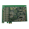
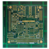
4-layer ENIG FR4 PCB is engineered for applications requiring robust current-carrying capacity and precise circuit routing, such as industrial power supplies, automotive control modules, and high-power electronic devices. The 2OZ (70μm) copper thickness on both outer layers enables it to handle high currents (up to 15A per trace) while minimizing voltage drop and heat generation—critical for power-hungry components like MOSFETs, IGBTs, and power inductors. The 3mils (75μm) minimum line width/space allows for dense circuit layouts, balancing high-power capability with compact design requirements.
Constructed from FR4 material with a 1.6mm thickness, the PCB offers a stable mechanical foundation and reliable electrical insulation (dielectric constant εr=4.5), suitable for both commercial and industrial environments. The ENIG (Electroless Nickel Immersion Gold) surface treatment with 2.5u” (0.06μm) gold thickness provides an oxidation-resistant finish that enhances solderability and withstands repeated soldering processes. The nickel underlayer (3-5μm) adds durability, making it ideal for high-reliability applications where contact resistance must remain stable over time.
The manufacturing process combines precision and performance:
- Laser Direct Imaging (LDI) ensures 3mils line/space accuracy, even for complex power/ground plane designs.
- Electrolytic copper plating achieves uniform 2OZ thickness, verified by cross-sectional analysis.
- 100% AOI inspection identifies surface defects, while flying probe tests verify electrical continuity.
- Thermal stress testing confirms the PCB’s ability to withstand reflow temperatures up to 260°C.
Engineers will appreciate the board’s versatility: its 4-layer structure (2 signal layers + 2 power/ground planes) simplifies impedance control for mixed-signal designs, while the thick copper supports heat dissipation in high-power circuits. In industrial automation, it excels in motor control panels exposed to vibration and temperature fluctuations; in automotive systems, it meets AEC-Q200 requirements for reliability in under-hood environments.
By choosing this 4-layer ENIG PCB, customers gain a solution that balances high-current capability with fine-line precision. Its combination of 2OZ copper, 3mils routing, and premium ENIG finish makes it a strategic choice for applications where power density, space efficiency, and long-term reliability are non-negotiable. Backed by ISO 9001:2015 certification and IPC-6012 Class 2 compliance, this PCB ensures consistent performance from prototype to mass production.