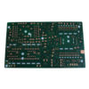
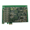
This 12-layer HDI PCB redefines high-density electronic integration, combining FR4 TG180 material with complex blind via structures to enable next-generation device miniaturization. The FR4 TG180 substrate (glass transition temperature 180°C) ensures thermal stability in high-power applications, while the 2.0mm thickness balances mechanical rigidity with layered routing complexity. The board’s 12-layer architecture supports a mix of signal, power, and ground planes, optimized for high-speed digital signals and dense BGA component placement.

Advanced Blind Via Engineering

  • Multi-Level Blind Vias:
    • L1-L3 & L1-L4: Top-layer blind vias enable direct connection to inner signal layers, reducing via stub length for 5G and RF applications.
    • L7-L12 & L9-L12: Bottom-layer blind vias support backside component routing, critical for 3D package-on-package (PoP) designs.
  • 0.2mm Microvia Precision:
    Laser-drilled vias with ±10μm accuracy, filled with conductive epoxy and plated to create airtight connections—eliminating voids in high-reliability scenarios.

HDI Manufacturing Excellence

  • Sequential Lamination Process:
    1. Core layers (L1-L12) laminated in stages with semi-additive processing (SAP) for 5μm trace resolution.
    2. Build-up layers added via electroless copper plating for fine-pitch routing (40μm line/space).
  • ENIG Surface Finish:
    • Nickel: 3-5μm for corrosion resistance
    • Gold: 0.05-0.1μm for long-term solderability and wire bond compatibility
  • Thermal Management:
    Thermal vias connecting power planes to outer layers, reducing hotspots in high-current sections (e.g., DC-DC converters).

High-Reliability Applications

  • Aerospace Avionics:
    Supports MIL-STD-202 environmental testing for vibration (20-2000Hz) and temperature (-55°C to +125°C).
  • Medical Imaging Devices:
    Low-loss dielectric properties (Dk=4.5, tanδ=0.02) minimize signal distortion in MRI or ultrasound equipment.
  • 5G Base Stations:
    Impedance-controlled layers (50Ω ±8%) for mmWave antenna arrays and high-speed data interfaces.

Quality Assurance & Compliance

  • 3D AOI Inspection:
    Verifies blind via registration and solder mask coverage on all 12 layers.
  • X-Ray Tomography:
    Confirms internal via integrity and layer alignment with <50μm tolerance.
  • Standards Met:
    • IPC-6012 Class 3 for mission-critical applications
    • RoHS/REACH compliant for lead-free manufacturing

PCB Capability


Item Standard PCB Customized PCB
Number of Layers 2-20 2-50
Material FR4 Hi Speed material from Taiwan Union, SY Tech, High Frequency material from Rogers etc.
PCB thickness 0.4-3.2mm 0.4-6.4mm
Copper Weight HOZ-3OZ HOZ-10OZ
Min. Hole Diameter 0.3mm 0.1mm by Laser Drill
PCB Size Min. 6.00X6.00mm Max. 600.00X620.00mm
PCB Finish HAL, HAL-leadfree, ENIG, ENEPIG, Immersion Tin, Immersion Silver, OSP
Min.Soldermask Dam. 4mils for 1OZ 2.5mils for 1OZ
Prepreg Type 2116,1080 2116,1080,7628,3313,106
Min.Width/Space 4/4 mils 2.5/2.5 mils
Min. Annular Ring 4/4 mils 2.5/2.5 mils
Aspect Ratio 8:1 15:1
Lead Time 2 weeks 5 Days - 5 Weeks
Impedance Tolerance ±5% - ±10% ±5% - ±10%
Other Techniques Gold fingers, Blind and Buried Holes, Peelable solder mask, Edge plating, Carbon Mask, Countersink hole,
Half/Castellated hole, Press fit hole, Via plugged/filled with resin, Via in pad (VIP, POFV), Multi-finishes on one PCB

This will close in 0 seconds

PCBA Capability


No. Item Process Capability Parameter
1 Order Quantity More than 1pcs
2 PCB Type Rigid PCB, FPC, Rigid-flex PCB
3 Assembly Tech SMT, THT, Mixed Tech or POP
4 Component Sourcing Full Turnkey, Partial Turnkey, Consigned
5 PCB Size 45*45mm -- 510*500mm
6 BGA Package BGA Dia. 0.14mm, BGA 0.2mm pitch
7 Parts Presentation Tape, Reel, Stick or Tray
8 Wire & Cable Wire harness and Cable Assembly
9 Quality Inspection Visual, SPI, FAI, AOI; X-RAY checking
10 Mounting Accuracy ±0.035mm (±0.025mm)
11 Min Package 01005 (0.4mm*0.2mm)
12 Conformal Coating Available by machine
13 IC Inspection Function, Electrical or Decap Test
14 Lead Time 3 days - 5 Weeks
15 Other Techniques Box Build Assembly, IC programming, Components cost-down, Function & aging test as custom,
Press fit assembly, SAC305 or better Solder Paste used, BGA reballing or rework,
Shield cover assembly for EMI emission control

This will close in 0 seconds

FPC Capability


No. Item Process Capability Parameter
1 Layer Count 1-8 Layers
2 FPC Material PI, PET, PEN, FR-4
3 Final Thickness 0.06-4.0mm
4 Board Size 250.00X1200mm
5 Copper Foil 12um,18um,35um,70um
6 Min width/Space 3mil/3mil
7 Holewall Copper Thickness 8-20μm
8 Surface Treatment HAL leadfree, ENIG, Immersion Silver/Tin, OSP
9 Outlines Dimension ±2mils
10 Solder Heat Resistance 280℃ / 10secs
11 Stiffener Type PI, FR4, Stainless Steel, Aluminum
12 Min. Hole Dia (PTH) 0.1mm±3mils
13 Min. Hole Dia (NPTH) 0.25±2mils
14 Max/Min Soldermask Thickness 2mil/0.5mil (50um/12.7um)
15 Min Slot 0.8mm×1mm

This will close in 0 seconds