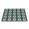
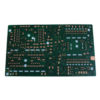
14-layer heavy copper PCB is designed for demanding applications that require exceptional current-carrying capacity and thermal management, such as industrial power supplies, renewable energy inverters, and high-power automotive systems. Constructed with FR4 High Tg170 material (glass transition temperature 170°C), the PCB withstands prolonged exposure to high temperatures without compromising mechanical or electrical properties. The 3.5mm board thickness provides rugged structural integrity, making it suitable for environments with vibration or mechanical stress, while the 14-layer architecture (typically 8 signal layers + 6 power/ground planes) enables complex routing for high-density, mixed-signal designs.
The defining feature is 3OZ (105μm) copper thickness in all layers, which supports current loads up to 30A per trace—ideal for power-hungry components like IGBTs, power MOSFETs, and large inductors. This heavy copper construction minimizes resistive heating and voltage drop, critical for maintaining efficiency in high-power circuits. The 0.5mm minimum hole diameter accommodates through-hole components and vias for thermal conduction, while the ENIG (Electroless Nickel Immersion Gold) surface treatment ensures reliable solderability and corrosion resistance. The nickel layer (3-5μm) provides durability, and the gold layer (0.05-0.1μm) protects against oxidation, making it suitable for long-term use in harsh environments.
Manufacturing this PCB involves advanced techniques to ensure precision and quality:
- DFM (Design for Manufacturability) analysis optimizes layer stacking and via placement to prevent thermal stress and maximize copper utilization.
- Laser drilling achieves 0.5mm holes with ±10μm accuracy, essential for maintaining via integrity in thick boards.
- Electrolytic copper plating ensures uniform 3OZ thickness across all layers, verified by cross-sectional analysis.
- Impedance control (optional for signal layers) maintains consistent performance for high-speed interfaces.
- 100% AOI (Automated Optical Inspection) and X-ray verification of internal layers ensure defect-free production.
Engineers will appreciate the PCB’s ability to handle both high-power and high-reliability requirements. In industrial applications, it excels in motor drives and control panels, where heat dissipation and current stability are critical. In renewable energy systems, the heavy copper layers support efficient power conversion in inverters and battery management systems. The High Tg170 material ensures the PCB remains stable in under-hood automotive environments or industrial machinery exposed to continuous operation at elevated temperatures.
By choosing this 14-layer heavy copper PCB, customers gain a solution that balances extreme power capability with design flexibility. Its combination of 3OZ copper in all layers, 3.5mm thickness, and ENIG finish makes it a strategic choice for applications where power density, thermal management, and long-term reliability are non-negotiable. Backed by IPC-6012 Class 2/3 compliance (optional) and rigorous thermal cycling tests, this PCB ensures consistent performance from prototype to mass production in the most demanding high-power electronic systems.

")