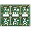
8-layer FR4 PCB is engineered for high-density electronic designs that require a balance of signal integrity, power distribution, and compact form factors, such as consumer electronics, medical devices, and industrial control modules. The 8-layer architecture (typically 4 signal layers + 4 power/ground planes) enables complex routing for fine-pitch components while minimizing electromagnetic interference (EMI). The 1.2mm board thickness offers a lightweight yet rigid foundation, ideal for space-constrained applications where weight and durability are critical.
Constructed with FR4 material, the PCB provides reliable electrical insulation (dielectric constant εr=4.5) and mechanical stability, suitable for a wide range of operating environments. The 2OZ (70μm) copper thickness on all layers enhances current-carrying capacity (up to 15A per trace) while maintaining design flexibility for both power and signal traces. The Green LPI (Liquid Photoimageable) solder mask not only protects the circuitry from environmental damage but also improves visual inspection accuracy, while the White silkscreen ensures clear component marking and designations for assembly and maintenance.
A key feature is the ENIG (Electroless Nickel Immersion Gold) surface treatment, which provides a smooth, corrosion-resistant finish for excellent solderability. The nickel layer (3–5μm) adds durability, and the gold layer (0.05–0.1μm) prevents oxidation, making it suitable for long-term use. The POFV (Plated Over Filled Vias) technology further enhances the PCB’s reliability: vias are filled with conductive material and plated over, eliminating voids that could cause thermal stress or solder wicking. This is particularly important for high-density designs with fine-pitch components (e.g., 0.5mm pitch BGAs) and ensures consistent performance in reflow soldering processes.
Manufacturing this PCB involves advanced techniques to ensure precision and quality:
- Laser Direct Imaging (LDI) achieves fine-line accuracy (minimum line width/space: 50μm/50μm) for complex routing.
- POFV processing uses conductive epoxy or resin to fill vias, followed by plating to create a smooth surface.
- 100% AOI (Automated Optical Inspection) verifies solder mask coverage and silkscreen clarity.
- Electrical testing ensures continuity and isolation resistance, meeting IPC-6012 Class 2 standards.
Engineers will appreciate the PCB’s versatility in handling both high-density signal routing and moderate power applications. In consumer electronics, it supports compact designs for smartphones, tablets, and wearables, where space is at a premium. In medical devices, the POFV technology and ENIG finish contribute to long-term reliability in diagnostic equipment. In industrial systems, the 2OZ copper and FR4 material provide the durability needed for control panels and automation modules.
By choosing this 8-layer FR4 PCB with 2OZ copper, ENIG finish, and POFV technology, customers gain a solution that balances density, reliability, and cost-effectiveness. Its combination of advanced via filling, premium surface treatment, and precise manufacturing makes it a strategic choice for applications where component integration and long-term performance are essential. Backed by ISO 9001:2015 certification, this PCB ensures consistent quality from prototyping to mass production.

")