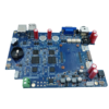
This 2-layer FR4 PCBA (Printed Circuit Board Assembly) is engineered for miniature electronic devices that demand a balance of reliability, conductivity, and assembly precision, such as wireless modules, wearable electronics, and medical sensors. With dimensions of 40mm×25mm and a 1.6mm thickness, the board maximizes space efficiency while supporting dense surface-mount component placement. Constructed from FR4 material, it offers consistent electrical insulation and mechanical stability, suitable for commercial-grade applications with moderate temperature and humidity ranges.
The 1OZ (35μm) copper thickness on both layers optimizes signal integrity and current-carrying capacity (up to 8A per wide trace), ideal for battery-powered devices. The Red LPI solder mask provides a durable, moisture-resistant coating that protects circuitry while enabling visual differentiation in multi-board assemblies, while the White silkscreen ensures clear component marking for quality control and maintenance. The ENIG (Electroless Nickel Immersion Gold) surface finish creates a corrosion-resistant, solder-friendly surface (3–5μm nickel, 0.05–0.1μm gold), ensuring reliable connections for fine-pitch components (down to 0.3mm pitch).
- Component Support:
- 01005 to 1206 passive components
- QFP, BGA (0.5mm pitch), and 0201 ultra-small packages
- Height restriction: ≤5mm for vertical clearance
- Assembly Processes:
- Lead-free reflow soldering (peak temperature: 260°C)
- Automated optical inspection (AOI) for solder joint quality
- X-ray inspection for BGA/CSP components
- Testing Options:
- In-circuit testing (ICT) for component functionality
- Functional testing (FT) per customer specifications
- Production Efficiency:
- 20 identical boards per panel reduce material waste by 30%
- Breakaway tabs with V-cut scoring for easy depaneling
- Cost Optimization:
- Economies of scale for high-volume orders (10k+ units)
- Shared setup costs across panels
- Assembly Compatibility:
- Compatible with standard pick-and-place machines (e.g., Yamaha, Juki)
- Supports tape-and-reel component feeding
- Material Traceability:
- RoHS-compliant components (lead-free, halogen-free)
- UL 94V-0 flammability rating for FR4
- Reliability Testing:
- Thermal cycling (-40°C to +85°C, 100 cycles)
- Humidity testing (85°C/85% RH, 1,000 hours)
- Standards Met:
- IPC-A-610 Class 2 for general electronics
- ISO 9001:2015 quality management system
- Wireless Communication:
Bluetooth/Wi-Fi modules for IoT gateways and smart home devices
- Medical Diagnostics:
Portable health monitors with compact sensor interfaces
- Consumer Electronics:
Wearable fitness trackers and hearables with space-constrained designs
- Industrial Sensors:
Compact environmental sensors for predictive maintenance
By choosing this 2-layer FR4 PCBA, engineers gain a fully assembled solution that balances precision SMT placement, ENIG reliability, and panelized production. The red solder mask offers visual differentiation in complex systems, while the 4×5 panel format ensures cost-effective scaling from prototype to mass production. Backed by comprehensive testing and compliance, this PCBA delivers consistent performance for applications where size, cost, and quality are critical.

")